1
The mask is a key consumable in the photolithography process.
The main processes in semiconductor wafer manufacturing include wafer preparation, pattern transfer, material doping, deposition, etching, and packaging.
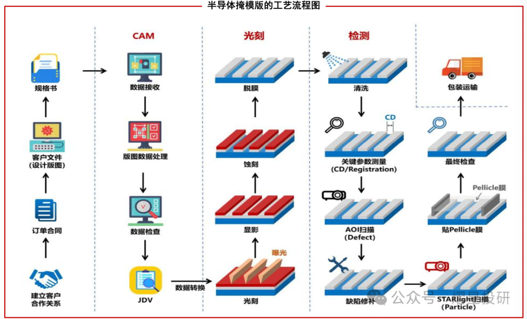
The photolithography process is the core procedure in semiconductor manufacturing, which includes: incoming material cleaning, drying, HDMS adhesion promotion, cold plate, pre-coating baking, cold plate, edge trimming, exposure, post-baking, cold plate, developing, cleaning, and hardening. The photolithography process leaves a photoresist with fine geometric structures on the substrate through the above processes, and then transfers this structure to the substrate through etching and other processes.
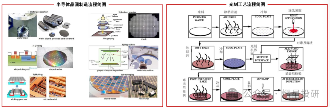
The role of the mask is to transfer the circuit patterns it carries onto silicon wafers and other substrate materials through exposure, thus achieving mass production of integrated circuits.
Semiconductor devices and structures are formed layer by layer through the production process. The chip design layout typically consists of dozens of layers of patterns, and the most critical step in chip manufacturing is to accurately transfer the patterns from each layer of the mask onto the wafer through multiple photolithography processes.
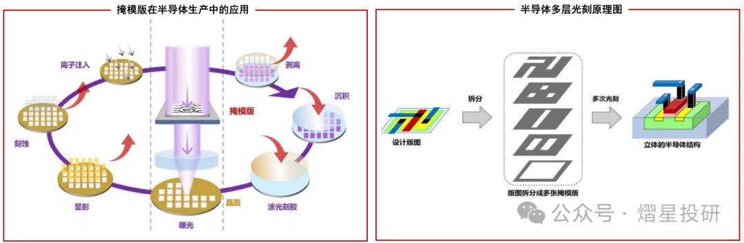
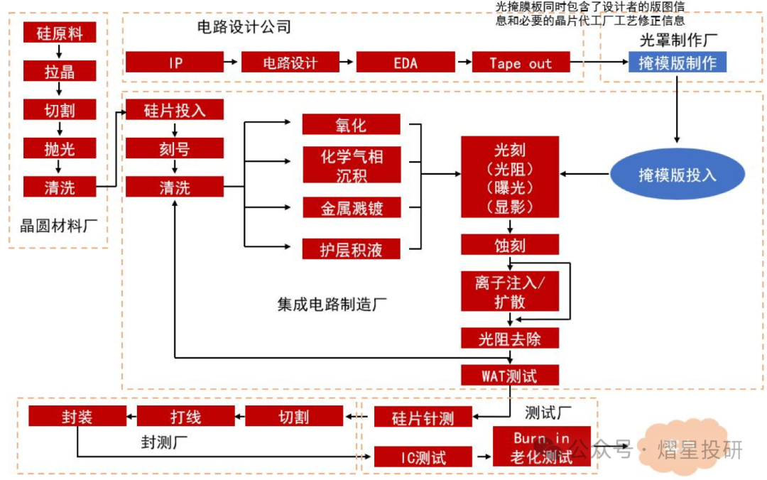
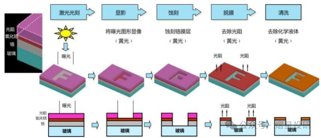
The semiconductor photolithography process requires a complete set of “photo-copying” masks with specific patterns that can be accurately aligned with each other, similar to the “film” of a traditional camera. The mask is one of the most critical materials in the semiconductor manufacturing process, and its quality directly affects the final product’s quality and yield. The photolithography process transfers the IC patterns from the mask onto the photoresist on the semiconductor substrate through exposure and developing processes, and then uses the formed resist pattern as a masking layer to block etching of the substrate during the etching process, to prevent impurities from diffusing into the substrate during the diffusion process, to block ion implantation during the injection process, and to block the etching of the metal film during the metallization process, thus making the mask indispensable in semiconductor planar processes.
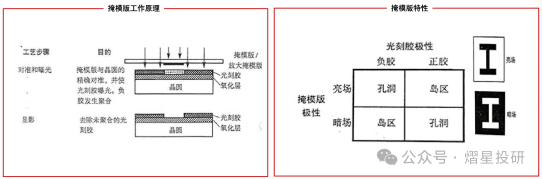
The mask design has both clear and dark field types, which can be selected based on the needs during exposure with photoresist (positive or negative). According to the Rayleigh criterion followed by photolithography technology, reducing the wavelength of the incident light source is one of the effective methods to improve the resolution of the photolithography system. However, the wavelength of the light source is not linearly selectable. For example, ASML has developed from g-line lithography machines to DUV lithography machines and now to EUV lithography machines. In DUV lithography machines, 249nm and 193nm are the most common wavelengths, while the light source wavelength for EUV lithography systems is 13.5nm. However, as time goes on, the size of chips shrinks exponentially, leading to an increasing gap between the specific light source wavelength and the size of the transistors to be imaged, causing physical diffraction to blur the image. When the critical dimensions of the chip are smaller than the wavelength of the light source, the required masks become increasingly complex.
2
Overview of the Mask Industry
From the perspective of the industrial chain, the mask industry is located upstream of the electronic information industry, and masks are one of the core materials in the manufacturing processes of downstream industries such as flat panel displays, semiconductors, and touch screens.The development of the mask industry is closely related to the development of its downstream industries, and the continuous growth of the downstream market size also provides a broader market space for the mask industry.
According to SEMI statistics from 2021, as an important component of semiconductor materials, masks account for about 12% of the semiconductor materials market size, second only to wafers and electronic specialty gases.
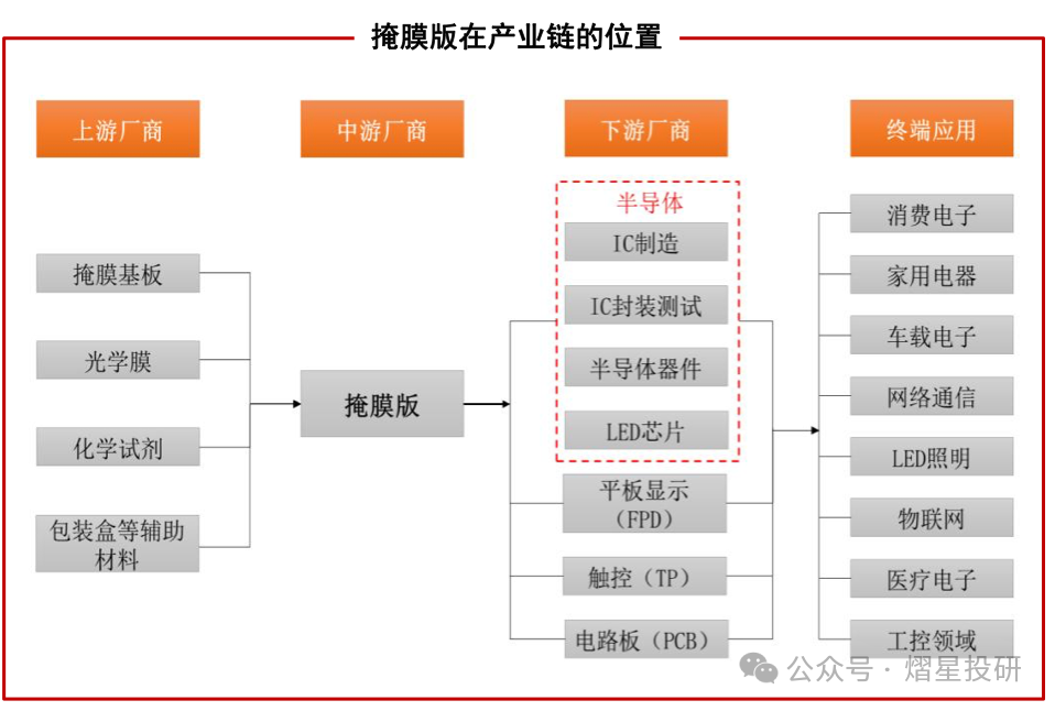
Masks are used in the production of semiconductors, display panels, touch screens, and circuit boards. From the perspective of downstream applications, mask ICs and semiconductors account for the largest share of usage in the flat panel display field. According to statistics from the Huajing Industry Research Institute, in the downstream segmentation of masks, 60% of the share is for ICs, 23% for LCDs, 5% for OLEDs, and 2% for PCBs.
According to statistics from the semiconductor industry organization SEMI,the global semiconductor materials market revenue is expected to reach $67.5 billion in 2024, achieving a year-on-year growth of 3.8%, but still below the peak in 2022.SEMI stated that the overall recovery of the semiconductor market and the increased demand for advanced materials in HPC and HBM manufacturing support the growth of material revenue in 2024.
SEMI divides semiconductor materials into two major areas: wafer manufacturing materials and packaging materials. The former is expected to achieve $42.9 billion in revenue in 2024, with a year-on-year growth of 3.3%; the latter is expected to reach $24.6 billion, with a year-on-year growth of 4.7%.
According to the 2024 annual report statistics from Lu Wei Optoelectronics,based on comprehensive assessments of demand from multiple institutions, the global market size for semiconductor masks is expected to reach $8.94 billion in 2025, with $5.788 billion for wafer manufacturing masks, $1.4 billion for packaging masks, and $1.75 billion for masks for other devices; the domestic semiconductor mask market size is expected to be around 18.7 billion RMB in 2025, with wafer manufacturing masks expected to be 10 billion RMB, packaging masks expected to be 2.6 billion RMB, and masks for other devices expected to be 6.1 billion RMB.
The semiconductor mask industry is characterized by significant capital investment, high technical barriers, and a strong reliance on proprietary technology.
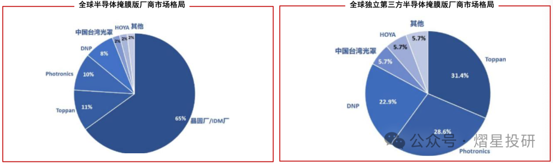
Wafer manufacturers set up their own mask factories mainly due to considerations of production capacity. However, as the process technology matures and the production levels of third-party mask manufacturers continue to improve, the many disadvantages of self-built mask factories gradually become apparent, such as huge equipment and labor investments, overly complex production processes, and excessively high costs. Third-party semiconductor mask manufacturers can fully leverage their technological specialization and economies of scale, providing significant scale economic effects. Given that the technical level and product performance indicators meet the requirements, the attractiveness of independent third-party mask manufacturers to wafer manufacturers is continuously increasing. According to SEMI data, in the global semiconductor mask market, wafer manufacturers’ self-built mask factories account for 65%, while independent third-party mask manufacturers account for 35%. Among them, the independent third-party mask market is mainly controlled by three companies: Photronics from the USA, Toppan from Japan, and DNP from Japan. Together, they account for over 80% of the market size, indicating a high market concentration.
Due to the high entry barriers of the semiconductor mask industry, the main domestic semiconductor mask manufacturers includeSMIC Mask Factory, DSW, Zhongwei Mask, Longtu Mask, QY Optoelectronics, and Lu Wei Optoelectronics.SMIC Mask Factory is a self-built factory for wafer manufacturing, supplying products for internal use; DSW is a subsidiary of China Resources Microelectronics. Currently, the overall revenue scale of domestic semiconductor mask manufacturers is relatively low, and their penetration rate is very low.
3
Overview of Listed Companies in the Mask Industry
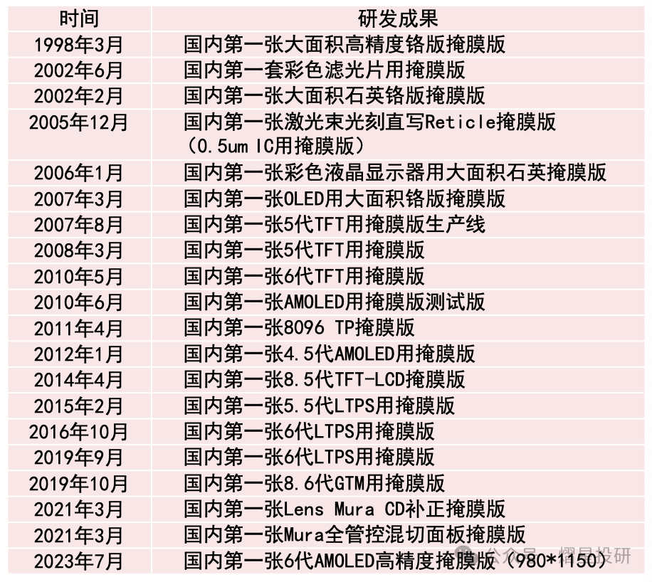
1. QY Optoelectronics: The earliest established leading manufacturer of masks in China.
The company was established on August 25, 1997, and is one of the earliest and largest mask production enterprises in China.
The company’s business mainly includes two major segments: flat panel display masks and semiconductor chip masks. In 2024, the company’s revenue from flat panel display masks was 859 million RMB, a year-on-year increase of 17.59%, of which the revenue from AMOLED/LTPS reached 361 million RMB, a year-on-year increase of 21.75%; in 2024, the company’s revenue from semiconductor chip masks was 193 million RMB, a year-on-year increase of 33.98%.
2. Lu Wei Optoelectronics
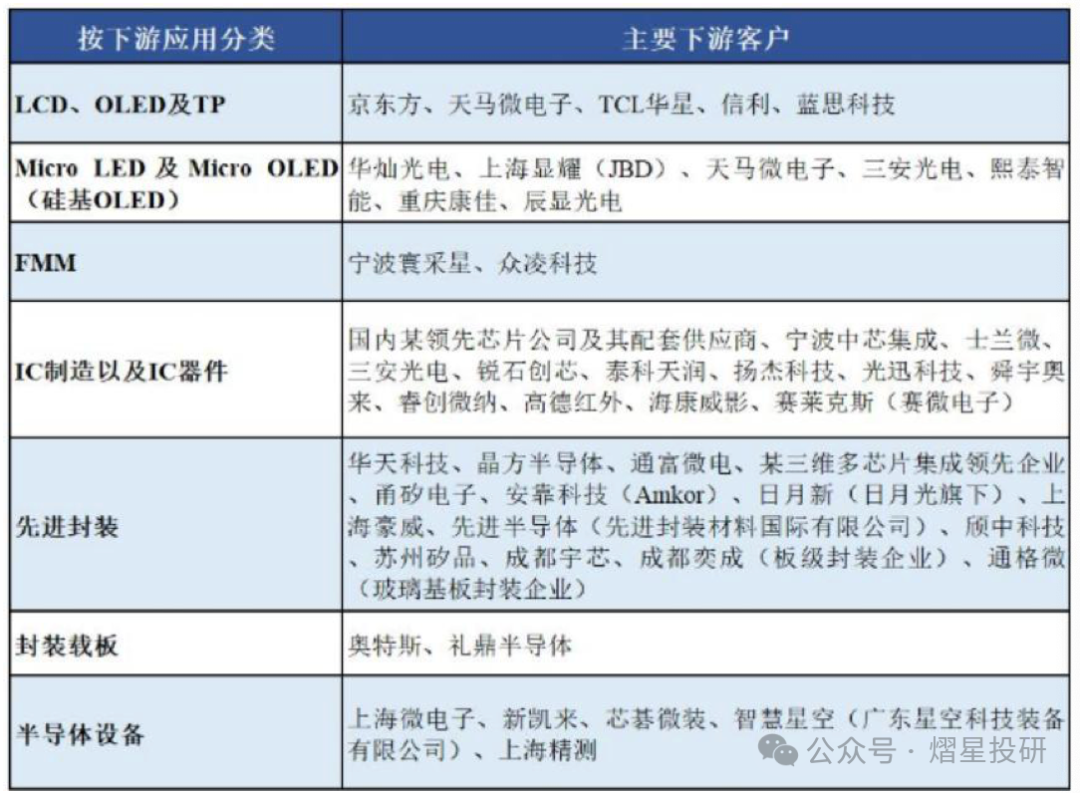
The company was established on March 26, 2012, and has been dedicated to the research, production, and sales of masks since its inception. Its products are mainly used in flat panel displays, semiconductors, touch screens, and circuit boards, serving as the benchmark and blueprint for transferring patterns in downstream microelectronics manufacturing processes.
With deep industry insights and professional R&D capabilities, the company has built a rich product matrix. In the display field, the company’s display masks have achieved full-generation coverage (G2.5-G11) and full technology coverage (LCD, AMOLED, LTPS, LTPO, Mini-LED, Micro-LED, silicon-based OLED, masks for FMM, etc.); in the semiconductor field, the company’s semiconductor masks have been fully applied in IC manufacturing, 1C devices, advanced packaging, etc.; through investment in Lu Xin Semiconductor, the company has positioned its semiconductor masks at a leading level in China (28nm), further improving its layout in the semiconductor field. The company will continue to promote the iterative upgrade of mask technology to better meet downstream customer needs. The 130-28nm semiconductor mask project invested and constructed by the company has completed the main factory topping in June 2024 and will begin to gradually move in equipment in the fourth quarter of 2024, with its process node layout ranking among the top domestic manufacturers.
3. Longtu Mask
The company was established on April 19, 2010, and its main business is the R&D, production, and sales of semiconductor masks, making it a rare independent third-party semiconductor mask manufacturer in China.
The company closely follows the development path of domestic specialty process semiconductors, continuously conducting technological breakthroughs and product iterations. The mass-produced semiconductor masks correspond to the process nodes of downstream semiconductor products covering 130nm, and the third-generation mask PSM products for higher process nodes have been successfully developed and sent for customer verification. The company’s mask products are widely used in power semiconductors, MEMS sensors, I0 packaging, and analog I0 and other specialty process semiconductor fields, with end applications covering new energy, photovoltaic power generation, automotive electronics, industrial control, wireless communication, IoT, and consumer electronics.
In the first half of 2025, the Longtu Mask Zhuhai project will be successfully put into production, and the company’s third-generation mask PSM products will make significant progress. The company’s KrF-PSM and ArF-PSM will be sent to some customers for testing and verification, among which the 90nm node products have successfully completed the transition from R&D to mass production, and the 65nm products have begun sample verification. The company’s influence in high-end processes is further enhanced, and the downstream fields covered are more diverse. The project has an annual planned capacity of 18,000 pieces, and it is expected to achieve a production value of 540 million RMB after reaching full capacity. The Zhuhai company has already started small-scale production in the second quarter, and it is expected to gradually ramp up in the second half of 2025. The company will drive performance growth through a dual engine of “high-end process breakthroughs + customer structure upgrades.”
The company’s products have been certified by several well-known domestic wafer manufacturers, such as Huahong Grace, Xilinx, Silan Microelectronics, Lian Microelectronics, Yandong Microelectronics, New唐 Technology, BYD Semiconductor, Yuxin Semiconductor, Changfei Advanced, and Yangjie Technology, among others. These manufacturers represent a stable and high-quality customer resource advantage for the company. As the revenue in the 2024 annual report and the 2025 first quarter report is contributed by the Shenzhen company, the company’s revenue from masks for power devices accounts for over 60%, while other applications mainly include advanced IC packaging, MEMS sensors, optical devices, and third-generation semiconductors. With the successful production of the Zhuhai factory, the company’s products are expected to further expand into RF chips, MCU chips, DSP chips, CI chips, and other fields, and the product structure is expected to be further optimized.


More acquisition information
Scan the QR code below
Professional service team



MoreIndustry Research
Scan the QR code below
Professional service team