Common Mistakes in PCB Design: How Many Have You Made?
In the process of hardware circuit design, mistakes are inevitable. Have you made any rookie errors? The comment section is open for you.Below are the five most common design issues in PCB design along with their respective countermeasures.
01
Pin Errors
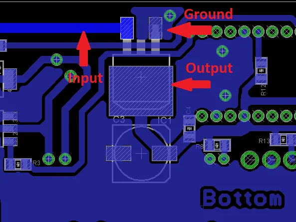
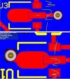
Linear voltage regulators are cheaper than switching power supplies but have lower energy transfer efficiency. Generally, many engineers choose to use linear voltage regulators due to their ease of use and cost-effectiveness.However, it is important to note that while they are convenient, they consume a lot of electrical energy, causing significant heat dissipation. In contrast, switching power supplies are more complex in design but offer higher efficiency.It is crucial to be aware that some voltage regulator output pins may be incompatible with each other, so it is necessary to confirm the relevant pin definitions in the chip manual before wiring.▲ Figure 1.1 A special pin arrangement of a linear voltage regulator
02
Wiring Errors
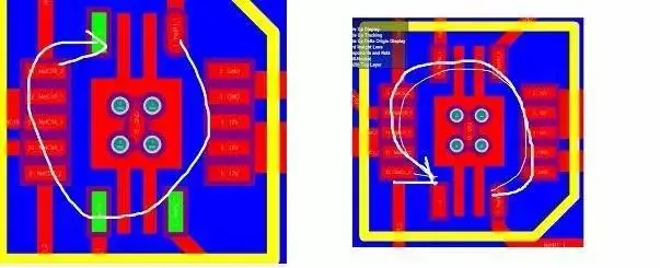
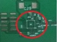
The differences between design and wiring are the main errors that occur in the final stage of PCB design. Therefore, it is essential to double-check certain aspects.For instance, component sizes, via quality, pad sizes, and review levels, etc. In summary, it is necessary to repeatedly confirm against the design schematic.▲ Figure 2.1 Line Inspection
03
Corrosion Traps
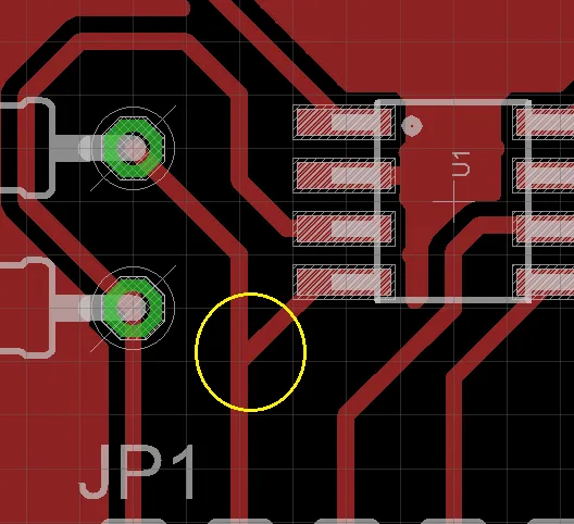
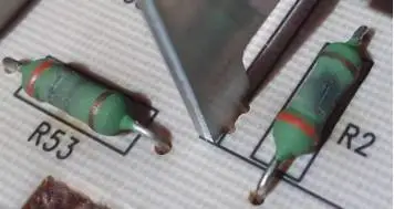
When the angle between PCB leads is too small (forming an acute angle), it can lead to the formation of corrosion traps (Acid Trap).These acute angle connections may retain corrosive liquid during the corrosion phase of the circuit board, thus removing more copper from that area, forming a trap.In the later stages, this may cause lead breakage, resulting in an open circuit. Due to modern manufacturing processes using photo-sensitive etching solutions, the occurrence of such corrosion traps has greatly reduced.▲ Figure 3.1 Connections forming acute angles
04
Component Tombstoning
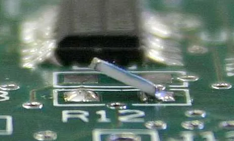
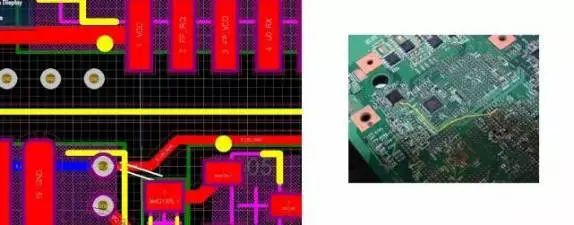
When soldering small surface-mount devices using reflow soldering, the devices may lift on one end due to solder’s wetting, commonly known as “tombstoning.”This phenomenon is usually caused by asymmetric wiring patterns, causing uneven heat distribution on the component pads. Proper DFM checks can effectively mitigate the occurrence of tombstoning.▲ Figure 4.1 Tombstoning phenomenon during PCB reflow soldering
05
Lead Width
When the current through PCB leads exceeds 500mA, the lead diameter may prove insufficient. Typically, surface traces carry more current than internal traces of multilayer boards because surface leads can dissipate heat through airflow.The trace width is also related to the thickness of the copper foil on the respective layer. Most PCB manufacturers allow you to choose copper foil thicknesses ranging from 0.5 oz/sq.ft to 2.5 oz/sq.ft.▲ Figure 5.1 PCB Lead WidthHere are some common mistakes that can easily happen:1. Did you reverse the pins for polarized capacitors in the schematic and PCB?2. Did you forget to connect power and ground… or connect them in reverse?3. Did you reverse the pin order of the connector?4. Did you reverse the RX and TX connections?5. Did you make a package based on assumptions, only to find that the component does not exist in that specification? Download the datasheet from Baidu, only to find that the component is unavailable.6. Did you directly copy a circuit, only to find the components are not available?Once, a team working on smart locks directly copied Samsung’s smart lock circuit, only to find that a capacitive touch button controller was made in Korea and was hard to purchase, with little agency support. They had to rely on their own experimentation and exploration.7. When selecting capacitors, did you only consider capacitance without considering voltage rating, resulting in a large package that cannot accommodate the required capacitor?8. When selecting resistors, did you only look at resistance value without considering power dissipation?9. After completing the PCB, did you ignore the DRC report, relying solely on visual inspection, only to find real issues after the board was returned?10. Did you make the package the wrong way?11. Did you fail to process the solder mask layer for heat dissipation pads?
Copyright Statement: The copyright of this article belongs to the original author and does not represent the views of the association. The articles promoted by the “Jiangxi Province Electronic Circuit Industry Association” are for sharing purposes only and do not represent the position of this account. If there are copyright issues, please contact us for deletion.