🔍See the article below for program acquisition methods
🔍The project includes complete programs, comments, references, and operation videos
⚡️Algorithm Simulation Effect Preview
The simulation test results using Vivado 2022.2 are as follows (217 convolution coding and decoding Verilog development, without using IP cores):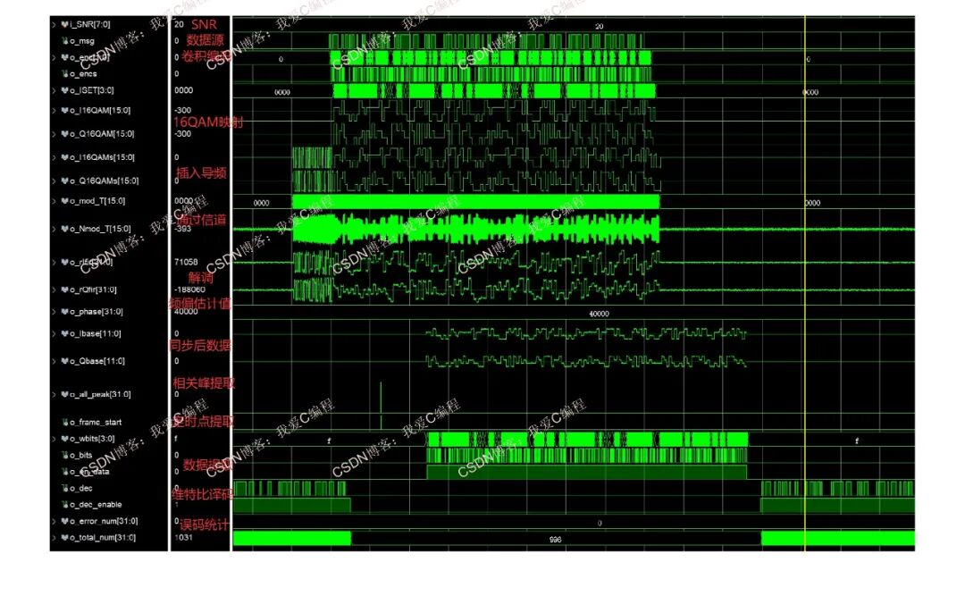
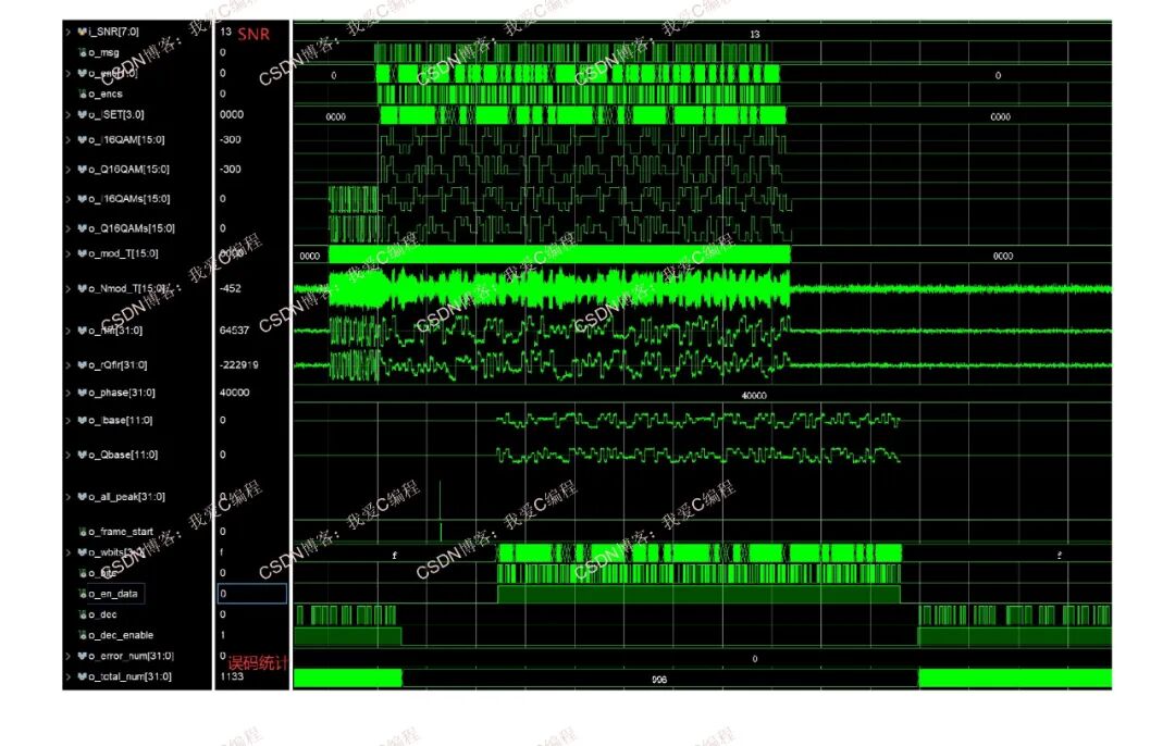
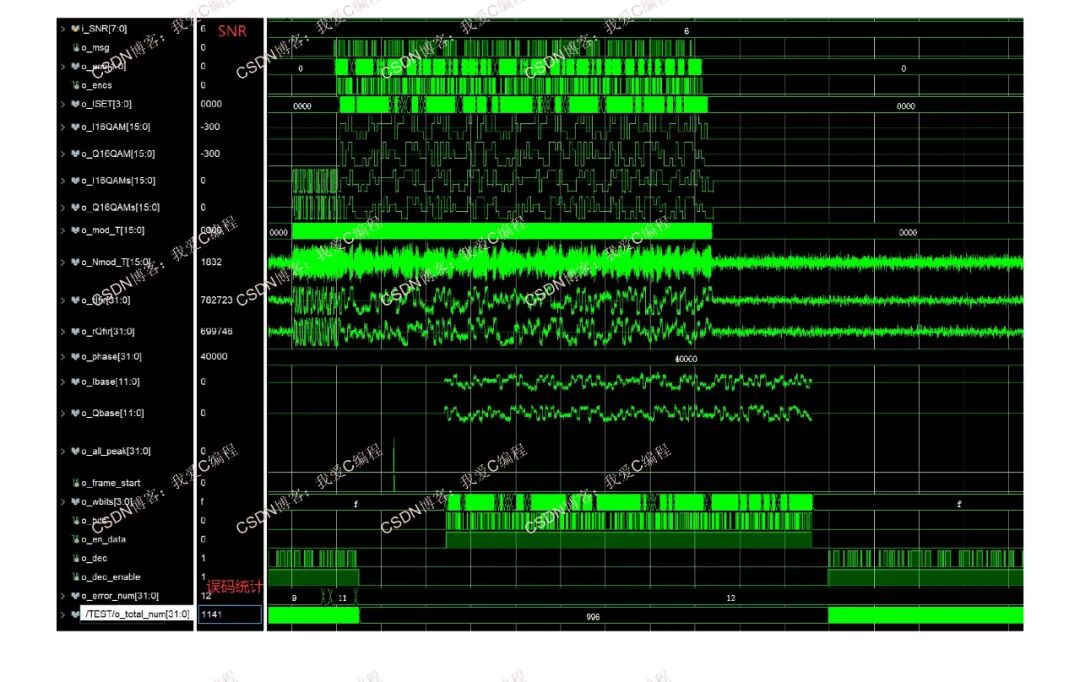
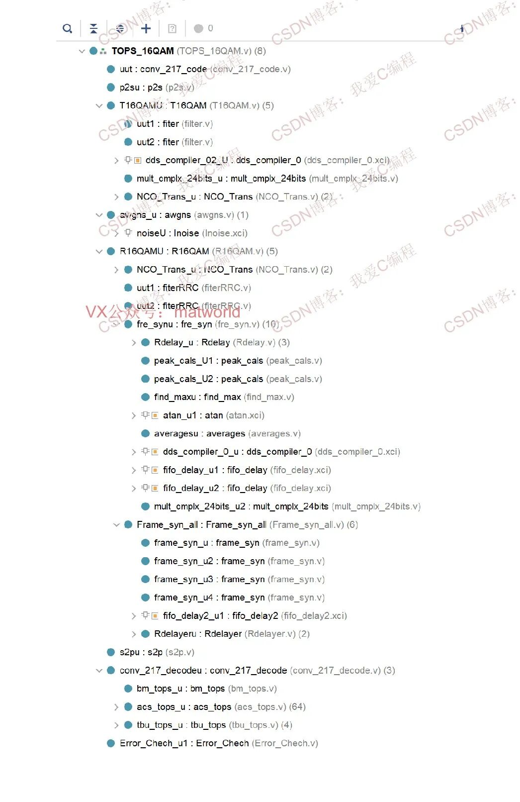
🚀System Overview
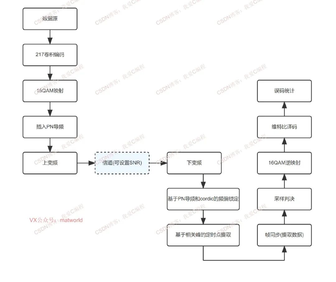
1. 217 Convolution Coding / Viterbi Decoding
The 217 convolution code is defined by the generator polynomial, with common generator polynomials being G1 = 111, G2 = 101, where the numbers represent the coefficients of the polynomial in binary form.
The convolution encoder: The encoding process is completed by the convolution encoder, which consists of multiple shift registers and programmable adders. Input data is sequentially passed through the shift registers, and then, according to the rules of the generator polynomial, performs modulo 2 addition with the delayed data to generate the encoded output.
Encoding rate: The 217 convolution code typically operates at a “2/7” encoding rate, meaning that every 2 input bits produce 7 encoded bits, increasing the redundancy of the data, allowing the receiver to detect and correct errors that occur during transmission.
Viterbi decoding is a maximum likelihood decoding algorithm for convolution codes. It estimates the most likely transmitted sequence among all possible sequences by calculating path metrics (such as Hamming distance) based on the received signal and the known convolution code generator polynomial, thereby correcting errors caused by noise during transmission and recovering the original input data.
2.16QAM Mapping / Inverse Mapping
16QAM is formed by superimposing two independent orthogonal 4ASK signals, where 4ASK is a signal obtained by modulating a carrier with multi-level signals. It is an extension of 2ASK modulation, and compared to 2ASK, this modulation has the advantage of a higher information transmission rate. Orthogonal Amplitude Modulation combines multi-level Amplitude Shift Keying (MASK) with orthogonal carrier modulation. The 16-level orthogonal amplitude modulation is a signal that combines amplitude and phase shift keying. There are two methods to generate 16QAM:
(1) Orthogonal Amplitude Modulation, which is formed by superimposing two orthogonal four-level amplitude shift keying signals;
(2) Composite Phase Shift Method: It is formed by superimposing two independent four-phase shift keying signals.
Here, the orthogonal amplitude modulation method is used. The digital signal is generated through the output port of the FPGA. In 16QAM modulation, each symbol contains 4 bits, so a 4-bit binary counter is needed to generate the digital signal. The output of the counter is mapped to a point on the constellation diagram, and then converted to an analog signal through a Digital-to-Analog Converter (DAC). The serial-to-parallel converter divides the binary symbol sequence at a rate of Rb into two paths, with a rate of Rb/2. The 2-4 level converter transforms the binary symbol sequence at a rate of Rb/2 into a 4-level signal at a rate of RS=Rb/log216, and the 4-level signal is multiplied by the orthogonal carrier to complete orthogonal modulation. After the two paths are superimposed, the 16QAM signal is produced. In the two paths of the binary symbol sequence at a rate of Rb/2, the output of the 2-4 level converter is a 4-level signal, i.e., M=16. After 4-level orthogonal amplitude modulation and superposition, 16 signal states are output, i.e., 16QAM.
The 16QAM signal is demodulated using the orthogonal coherent demodulation method. The demodulator first performs orthogonal coherent demodulation on the received 16QAM signal, multiplying one path by cosωct and the other by sinωct. Then, through a low-pass filter, the high-frequency components generated by the multiplier are filtered out, obtaining the useful signal. The output of the low-pass filter (LPF) can recover the level signal through sampling and decision-making.
3. Upconversion / Downconversion
The process of shifting the frequency spectrum of the baseband signal to the desired higher carrier frequency. The principle is to send the signal to be frequency-shifted and a fixed frequency local oscillator signal into a nonlinear device (mixer), obtaining two frequencies that are the sum and difference of the frequencies, and then filtering to extract the upper sideband signal, completing the upconversion, thus modulating the baseband signal onto a high-frequency carrier for transmission.
Downconversion is the reverse process of upconversion, which shifts the frequency spectrum of the received high-frequency signal down to a lower frequency, usually intermediate frequency or baseband frequency. Similarly, it is mixed with a sine signal generated by the local oscillator, and then the lower sideband signal (or further processed to obtain the baseband signal) is taken out for subsequent demodulation and other processing.
4. Frequency Offset Locking Based on PN Pilot
When the sender transmits data frames, a known pseudo-random (PN) pilot sequence is added. The receiver uses the PN pilot sequence to estimate the frequency offset of the signal. The receiver performs delay and conjugate multiplication on the received pilot data, and then uses the CORDIC algorithm for iterative rotation operations based on its real and imaginary parts to estimate the phase offset of the signal, thus obtaining the frequency offset value. Finally, by multiplying the received signal with a negative complex exponential function, frequency offset compensation is achieved, locking the frequency offset to zero.
5. Timing Point Extraction Based on Correlation Peaks
In the received signal, the timing point is determined by searching for correlation peaks with a locally known sequence (such as training sequence or pilot sequence). Specifically, the received signal is correlated with the local sequence, and when their phases and times align, the correlation value peaks, and this peak point corresponds to the best timing point, used to determine the sampling moment of the signal to ensure the accuracy of subsequent signal processing.
6. Frame Synchronization
In digital communication, information is usually organized and transmitted in frames. The purpose of frame synchronization is to determine the starting position of each frame so that the receiver can correctly demodulate the data within each frame. The structure of the transmitted frame is: frame synchronization code + information code sequence. The frame synchronization code is a code sequence with a specific pattern, used by the receiver to identify the start of the frame. The process of frame synchronization is to search for the position in the received sequence that matches the frame synchronization code. Once a matching position is found, the starting position of the frame is determined, and subsequent symbols can be correctly divided and processed according to the frame structure.
7. Sampling Decision
After determining the timing point, the received signal is sampled, and the sampled values are compared with the preset decision threshold. Based on the comparison results, the level value of the received signal is determined, thus recovering the original binary bit stream.
✨Some Core Code
..`timescale 1ns / 1ps//////////////////////////////////////////////////////////////////////////////////// Company: // Engineer: // // Create Date: 2024/08/05 03:30:02// Design Name: // Module Name: TOPS_8PSK// Project Name: // Target Devices: // Tool Versions: // Description: // // Dependencies: // // Revision:// Revision 0.01 - File Created// Additional Comments:// //////////////////////////////////////////////////////////////////////////////////

module TOPS_16QAM(input i_clk,input i_clkdx,input i_clkd2x,input i_rst,input signed[7:0]i_SNR,input[1:0]i_en,input i_dat,// Convolution encodingoutput [1:0]o_enc,output      o_encs,

output [3:0]o_ISET,output  signed[15:0]o_I16QAM,output  signed[15:0]o_Q16QAM,output signed[15:0]o_I16QAMs,output signed[15:0]o_Q16QAMs,output signed[15:0]o_mod_T,output signed[15:0]o_Nmod_T,

output  signed[31:0]o_rIfir,output  signed[31:0]o_rQfir,output signed[31:0]o_phase,// Demodulated I-channel baseband signal (11-bit signed)output signed[11:0]o_Ibase,output signed[11:0]o_Qbase,// Signal peak detection result (31-bit signed)output signed[31:0]o_all_peak,// Frame start flag (active high)output           o_frame_start,output[3:0]o_wbits, // Demodulated I-channel data bitoutput  o_bits,
// Demodulated data enable signaloutput  o_en_data, // Viterbi decoding outputoutput  o_dec,// Decoding enable signaloutput  o_dec_enable,output signed[31:0]o_error_num,// Error bit count (31-bit signed)output signed[31:0]o_total_num  // Total data bit count (31-bit signed)  );0sj4_001m
🌐How to Obtain the Complete Project
Method 1: Copy the link to the browser https://mbd.pub/o/bread/YZWZlptvZA==
Method 2: Click 【Read Full Article】 at the bottom left of the article

Method 3: If the above link is invalid, for program debugging bugs or project collaboration, please contact via WeChat or QQ.