Click the blue text to follow us

“From signal to melody, all it takes is a palm-sized FPGA signal generator.” This project is not just an electronic practice piece, but a miniature experimental platform that can “produce sound.” It is based on the “Little Foot” FPGA, capable of outputting sine waves, triangle waves, and square waves, with a frequency range covering 100Hz to 200kHz, precise amplitude adjustment, and even the ability to drive a buzzer to produce sound, while displaying waveform parameters in real-time and supporting PC-side LabVIEW/MATLAB interface control. With expertise in hand, one can play with the world of waveforms.

1. Project Requirements

Comprehensive topic – Create a signal generator that can be controlled by a host computer, with adjustable waveform, amplitude, and frequency output.
1. Capable of generating sine waves, triangle waves, and square waves, with waveform switching controlled by a toggle switch on the FPGA.2. The amplitude of the generated signal can be adjusted between 0-3Vpp, with a resolution of 10mV, adjustable via a potentiometer.3. The frequency of the generated signal can be adjusted between 100Hz – 200KHz, with a frequency adjustment resolution of up to 10Hz.4. Signals in the frequency range of 1KHz – 10KHz are sent to the buzzer simultaneously, driving the buzzer to produce sound; adjusting the frequency and amplitude of the signal will change the buzzer’s sound output.5. The generated waveform (as illustrated), its amplitude, and frequency are displayed in real-time on an OLED screen. A control interface can be written on the PC using LabVIEW, MATLAB, or other tools, allowing waveform, amplitude, and frequency parameters to be changed via the interface, with settings transmitted to the FPGA board via UART for waveform adjustment.6. Both PC control and board control are effective simultaneously.
2. Overall Module Schematic

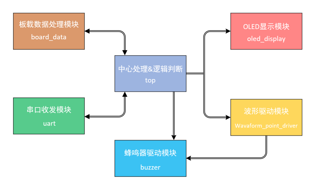
- Onboard data processing module: processes data from onboard buttons, toggle switches, and potentiometers, outputting control signal types (board_signal), signal frequency (three parameters: board_x10_n, board_1k_n, board_10k_n), signal amplitude (board_range), and UART ready-to-send flag signal (board_change_flag) to the top-level module.
- UART transceiver module: responsible for UART transmission and reception, primarily using ASCII code.
- OLED display module: responsible for displaying the current waveform type, frequency, and amplitude.
- Waveform driving module: responsible for outputting the currently calibrated control signal type, frequency, and amplitude as a 10-bit digital signal, and outputting the corresponding triangle wave (unmodulated) to the buzzer driving module.
- Buzzer driving module: responsible for driving the buzzer tone when the current frequency is in the range of 1k~10k, while introducing the amplitude value to adjust the buzzer’s pitch.
- Top-level module: responsible for scheduling various modules and controlling flag signals.

3. Onboard Data Processing Module and Physical Display

Mainly includesbuttons,toggle switches,rotary potentiometer data processing. The onboard control schematic is as follows:
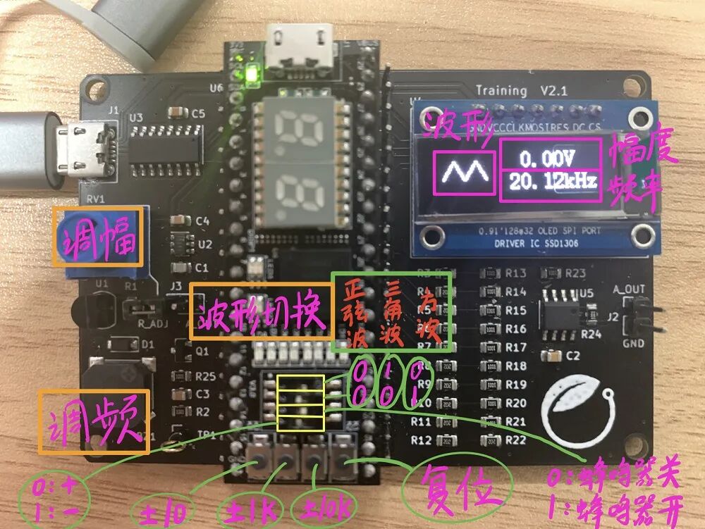
The buttons are defined from left to right asButton 1 ±10Hz,Button 2 ±1kHz,Button 3 ±10kHz, andReset button. Control is as shown in the figure above.
The driving code for the potentiometer and ADS7868 was directly referenced from the example code on the project page (Simple Voltmeter Design:https://www.eetree.cn/wiki/voltage_meter_sadc_verilog).
This module has two key points:
1. The three buttons and toggle switch control the frequency of the waveform.
2. Obtain the onboard data change flag (used to trigger UART transmission).
The code is as follows:
module board_data(    input clk,    input rst,    input [2:0]key,    input  [2:0]sw,
    input      dat,    // SPI bus SDA    output         cs,    // SPI bus CS    output       sclk,    // SPI bus SCK
    output  reg [1:0]board_signal,    output  reg [6:0]board_x10_n,    output  reg [3:0]board_x1k_n,    output  reg [4:0]board_x10k_n,    output  reg [7:0]board_range,
    output  reg board_change_flag);
    wire [2:0]key_pulse; // Instantiate debounce module    debounce #(.N(3)) u0(        .clk(clk),        .rst(rst),        .key(key),        .key_pulse(key_pulse)    );

    wire       adc_done;    wire  [7:0]adc_data;    wire adc_cs,adc_clk;       assign    cs   =  adc_cs;  assign    sclk =  adc_clk;    ADC7868_driver uadc(        .clk(clk),        .rst_n(rst),        .adc_cs(adc_cs),        .adc_clk(adc_clk),        .adc_dat(dat),        .adc_done(adc_done),        .adc_data(adc_data)    );
//---------------- Onboard data change flag judgment --------------------    reg [2:0]key_pulse_pre;    always @(posedge clk)        key_pulse_pre <= key_pulse;
    reg [2:0]sw_pre;    always @(posedge clk)        sw_pre <= sw;
    reg [16:0]cnt10ms;    always @(posedge clk or negedge rst) begin        if(!rst)            cnt10ms <= 17'd0;        else if(cnt10ms == 17'd120_000)            cnt10ms <= 17'd0;        else            cnt10ms <= cnt10ms + 1'b1;    end
    reg [7:0]board_range_gap;    reg [7:0]board_range_pre;    always @(posedge cnt10ms[16])        board_range_pre <= board_range;
    always @(posedge clk) begin        if(board_range_pre >= board_range)            board_range_gap <= board_range_pre - board_range;        else            board_range_gap <= board_range - board_range_pre;    end

    always @(posedge clk or negedge rst) begin        if(!rst)            board_change_flag <= 1'b0;                else if(key_pulse_pre != key_pulse)            board_change_flag <= 1'b1;        else if(sw_pre != sw)            board_change_flag <= 1'b1;        //else if(board_range_gap >= 8'd3)//board_change_flag <= 1'b1;        else            board_change_flag <= 1'b0;    end
// Waveform type selection (onboard)//reg [1:0]board_signal;    always @(*)case(sw[1:0])2'b00: board_signal <= 2'b00;2'b01: board_signal <= 2'b01;2'b10: board_signal <= 2'b10;default:;        endcase

// Waveform modulation factor (onboard)//reg [7:0]board_range; // Onboard button frequency adjustment logic carry borrow//reg [6:0]board_x10_n;//reg [3:0]board_x1k_n;//reg [4:0]board_x10k_n;    always @(posedge clk or negedge rst)        if(!rst) begin            board_x10_n <= 7'd10;            board_x1k_n <= 4'd0;            board_x10k_n <= 5'd0;        end        else begin            case({sw[2],key_pulse})                4'b0100: begin                    if(board_x10_n == 7'd99) begin        // + 10                                                if(board_x1k_n == 4'd9)begin                            if(board_x10k_n < 5'd20) begin                                board_x10_n <= 7'd0;                                board_x1k_n <= 4'd0;                                board_x10k_n <= board_x10k_n + 1'b1;endendelse begin                            board_x10_n <= 7'd0;                            board_x1k_n <= board_x1k_n + 1'b1;endendelse if(board_x10k_n < 5'd21)                        board_x10_n <= board_x10_n + 1'b1;end
4'b0010: begin                            //+ 1k                    if(board_x1k_n == 4'd9)     begin                        if(board_x10k_n < 5'd21) begin                            board_x1k_n <= 4'd0;                            board_x10k_n <= board_x10k_n + 1'b1;                        end                    end                    else if(board_x1k_n < 4'd9) begin                        if(board_x10k_n < 5'd21)                            board_x1k_n <= board_x1k_n + 1'b1;endend
4'b0001:                    if(board_x10k_n < 5'd20)                        board_x10k_n <= board_x10k_n + 1'b1;
                4'b1100: begin                    if(board_x10_n > 7'd10)                        board_x10_n <= board_x10_n - 1'b1;else begin                        if(board_x10_n == 7'd0)                            if(board_x1k_n == 4'd0)                                if(board_x10k_n == 5'd0)                                    ;                                else begin                                    board_x10k_n <= board_x10k_n - 1'b1;                                    board_x1k_n <= 4'd9;                                    board_x10_n <= 7'd99;endelse begin                                board_x1k_n <= board_x1k_n - 1'b1;                                board_x10_n <= 7'd99;endelse                            if(board_x1k_n == 4'd0 && board_x10k_n == 5'd0)                                ;else                                board_x10_n <= board_x10_n - 1'b1;                                        end                end
                4'b1010: begin                    if(board_x1k_n == 4'd0) begin                        if(board_x10k_n == 5'd0)                            ;else if(board_x10k_n > 5'd0)begin                            board_x10k_n <= board_x10k_n - 1'b1;                            board_x1k_n <= 4'd9;                        end                    end                    else if(board_x1k_n == 4'd1) begin                        if(board_x10k_n == 5'd0) begin                            if(board_x10_n >= 7'd10)                                board_x1k_n <= board_x1k_n - 1'b1;                        end                        else if(board_x10k_n > 5'd0)begin                            board_x1k_n <= board_x1k_n - 1'b1;                        end                    end                    else if(board_x1k_n >= 4'd2) begin                        board_x1k_n <= board_x1k_n - 1'b1;                    end                end
                4'b1001: begin                    if(board_x10k_n == 5'd1) begin                        if(board_x10_n >= 7'd10)                            board_x10k_n <= board_x10k_n - 1'b1;                        else if(board_x1k_n != 4'd0)                            board_x10k_n <= board_x10k_n - 1'b1;                                                end                    else if(board_x10k_n >= 5'd2) begin                        board_x10k_n <= board_x10k_n - 1'b1;                    end                end
                default: ;            endcase        end
// Waveform amplitude selection    always @(posedge clk or negedge rst) begin        if(adc_done == 1'b1)                board_range <= adc_data;    end
endmodule
4. UART Transceiver Module
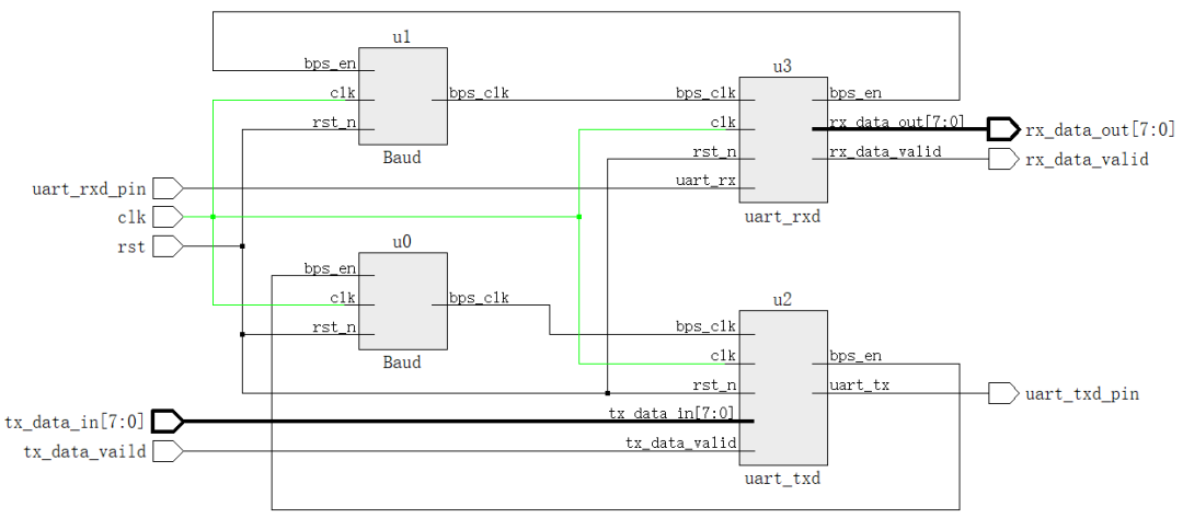
 The UART transceiver 1-byte driving code directly references the example code on the project page (Reference UART Monitoring System Design:https://www.eetree.cn/wiki/%E4%B8%B2%E5%8F%A3%E7%9B%91%E8%A7%86%E7%B3%BB%E7%BB%9F%E8%AE%BE%E8%AE%A1), and the following figure shows the RTL view of transmitting and receiving one byte of data.
This design is a signal generator that customizes the UART protocol.
-
1. Characters “s” / “t” / “q” represent sine wave/triangle wave/square wave respectively.
-
2. Character “F” represents frequency.
-
3/4/5/6/7. Characters “0”~”9″ represent the first five digits of the frequency value.
-
8. Character “U” represents amplitude.
-
9/10/11/12. Characters “0”~”3″ represent amplitude factors “——” “——” “——” “——” (high~low, two digits represent one character, totaling 8 digits, or 4 characters).
-
13. End character “$”.
The code is as follows:
module uart(    input clk,    input rst,    input uart_rxd_pin,    input txd_ready_flag,          // UART ready-to-send flag    input [1:0]uart_t_signal,      // Waveform name    input [6:0]uart_t_x10_n,    input [3:0]uart_t_x1k_n,    input [4:0]uart_t_x10k_n,    input [7:0]uart_t_range,       // Amplitude factor
    output uart_txd_pin,    output reg rxd_finish_flag,    // UART reception complete flag    output [1:0]uart_r_signal, // Waveform name    output [6:0]uart_r_x10_n,    output [3:0]uart_r_x1k_n,    output [4:0]uart_r_x10k_n,    output [7:0]uart_r_range   // Amplitude factor);
    //------------------ UART send and receive state machine ---------------------//-----------------------------------------------------------    reg [7:0]txd_state,txd_next_state;    localparam  // UART send state        txd_s1  = 8'b0000_0001,        txd_s2  = 8'b0000_0010,        txd_s3  = 8'b0000_0100,        txd_s4  = 8'b0000_1000,        txd_s5  = 8'b0001_0000,        txd_s6  = 8'b0010_0000,        txd_s7  = 8'b0100_0000,        txd_s8  = 8'b1000_0000;

    reg [4:0]rxd_state;            localparam  // UART receive state        rxd_s1  = 4'b0001,        rxd_s2  = 4'b0010,        rxd_s3  = 4'b0100,        rxd_s4  = 4'b1000;//-----------------------------------------------------------

//---------------- UART send byte interval counter ---------------------//-----------------------------------------------------------    reg    [7:0]byteinterval_cnt;  // UART send byte interval counter    reg         byteinterval_flag; // UART send byte interval flag signal    localparam  byte_interval = 8'd80;
// UART send interval counter counting control    always @(posedge clk or negedge rst) beginif(!rst)            byteinterval_cnt <= 0;else if(byteinterval_flag == 1'b1)            byteinterval_cnt <= byteinterval_cnt + 1'b1;else if(byteinterval_flag == 1'b0)            byteinterval_cnt <= 0;    end//------------------------------------------------------------

//-------------------- Instantiate data conversion module -----------------------//-----------------------------------------------------------    reg [1:0]rxd_signal;    reg [19:0]rxd_frequency;    reg [7:0]rxd_range;
    wire [7:0]txd_signal;    wire [19:0]txd_frequency;    wire [15:0]txd_range;
    wire [1:0]uart_r_signal0;    wire [6:0]uart_r_x10_n0;    wire [3:0]uart_r_x1k_n0;    wire [4:0]uart_r_x10k_n0;    wire [7:0]uart_r_range0;    assign uart_r_signal = uart_r_signal0;    assign uart_r_x10_n = uart_r_x10_n0;    assign uart_r_x1k_n = uart_r_x1k_n0;    assign uart_r_x10k_n = uart_r_x10k_n0;    assign uart_r_range = uart_r_range0;
serial_data_conversion uconversion(        // UART send data (before conversion)        .uart_t_signal(uart_t_signal),      // Waveform name        .uart_t_x10_n(uart_t_x10_n),        .uart_t_x1k_n(uart_t_x1k_n),        .uart_t_x10k_n(uart_t_x10k_n),        .uart_t_range(uart_t_range),       // Amplitude factor// UART receive data (before conversion)        .rxd_signal(rxd_signal),        .rxd_frequency(rxd_frequency),        .rxd_range(rxd_range),
// UART send data (after conversion)        .txd_signal(txd_signal),        .txd_frequency(txd_frequency),        .txd_range(txd_range),
// UART receive data (after conversion)        .uart_r_signal(uart_r_signal0), // Waveform name        .uart_r_x10_n(uart_r_x10_n0),        .uart_r_x1k_n(uart_r_x1k_n0),        .uart_r_x10k_n(uart_r_x10k_n0),        .uart_r_range(uart_r_range0)   // Amplitude factor    );//-----------------------------------------------------------

//------------------ Instantiate UART receive 1-byte module ---------------------//-----------------------------------------------------------    wire [7:0]rx_1byte_data;    reg  [7:0]tx_1byte_data;    reg  tx_data_valid;    wire rx_data_valid;    wire uart_tx_pin;    wire tx1byte_finish_flag;     // During transmission = 0  Transmission complete and idle time = 1    assign uart_txd_pin = uart_tx_pin;uart_1byte uart_1byte0(        .clk(clk),        .rst(rst),        .uart_rxd_pin(uart_rxd_pin),      // UART receive pin
        .rx_data_out(rx_1byte_data),      // UART received data        .rx_data_valid(rx_data_valid),    // UART received data flag        .tx_data_in(tx_1byte_data),       // Data to be sent via UART        .tx_data_vaild(tx_data_valid),    // UART ready-to-send pulse flag signal
        .uart_txd_pin(uart_tx_pin),        // UART send pin                .tx1byte_finish_flag(tx1byte_finish_flag)    );//-----------------------------------------------------------

//--------------------------- UART send protocol module ------------------------------------//-------------------------------------------------------------------------------    reg [2:0]nX4_flag;    reg tx_data_valid;    reg [7:0]tx_1byte_data;    reg [19:0]txd_f;    reg [15:0]txd_r;    always @(posedge clk or negedge rst) beginif(!rst) begin            txd_state <= txd_s1;            tx_data_valid <= 1'b0;            nX4_flag <= 3'd0;endelse begincase(txd_state)                txd_s1: beginif(txd_ready_flag) begin                        txd_r <= txd_range;                        txd_f <= txd_frequency;
                        tx_1byte_data <= txd_signal;  // s/t/q waveform type                        tx_data_valid <= 1'b1;                        txd_state      <= txd_s2;                        txd_next_state <= txd_s3;                    endelse begin                        tx_data_valid <= 1'b0;                        txd_state <= txd_s1;                        end                end
                txd_s2: txd_state <= txd_next_state;  // UART send buffer state                txd_s3: beginif(tx1byte_finish_flag) begin                        byteinterval_flag <= 1'b1; // Start interval counter flag signal (can be understood as delay)if(byteinterval_cnt >= byte_interval) begin  // Check if the byte interval counter has reached the requirement (the counter is counted in another always block)                            tx_1byte_data <= 8'd70;        // Assign the next data to be sent as 'F'                            tx_data_valid <= 1'b1;                   // Set send flag signal to 1                            txd_state <= txd_s2;                            txd_next_state <= txd_s4;                            byteinterval_flag <= 1'b0;                // Turn off byte interval counter flag signal                        end    else                            txd_state <= txd_s3;                    endelse begin                        tx_data_valid <= 1'b0;                        txd_state <= txd_s3;                    end                end
                txd_s4: beginif(nX4_flag >= 3'd5) begin                        txd_state <= txd_s5;                        nX4_flag  <= 3'd0;endelse beginif(tx1byte_finish_flag) begin                            byteinterval_flag <= 1'b1; // Start interval counter flag signal (can be understood as delay)if(byteinterval_cnt >= byte_interval) begin  // Check if the byte interval counter has reached the requirement (the counter is counted in another always block)                                tx_1byte_data <= {4'd3,txd_f[19:16]};    // Assign the next data to be sent                                txd_f <= txd_f << 4;                                tx_data_valid <= 1'b1;                   // Set send flag signal to 1                                txd_state <= txd_s2;                                                            byteinterval_flag <= 1'b0;                // Turn off byte interval counter flag signal                                                    txd_next_state <= txd_s4;                                nX4_flag <= nX4_flag + 1'b1;
                            end    else                                txd_state <= txd_s4;                        endelse begin                            tx_data_valid <= 1'b0;                            txd_state <= txd_s4;                        end                    end                end
                txd_s5: beginif(tx1byte_finish_flag) begin                        byteinterval_flag <= 1'b1; // Start interval counter flag signal (can be understood as delay)if(byteinterval_cnt >= byte_interval) begin  // Check if the byte interval counter has reached the requirement (the counter is counted in another always block)                            tx_1byte_data <= 8'd85;        // Assign the next data to be sent as 'U'                            tx_data_valid <= 1'b1;                   // Set send flag signal to 1                            txd_state   <= txd_s2;                            txd_next_state <= txd_s6;                            byteinterval_flag <= 1'b0;                // Turn off byte interval counter flag signal                        end    else                            txd_state <= txd_s5;                    endelse begin                        tx_data_valid <= 1'b0;                        txd_state <= txd_s5;                    end                end
                txd_s6: beginif(nX4_flag >= 3'd4) begin                        txd_state <= txd_s7;                        nX4_flag  <= 3'd0;endelse beginif(tx1byte_finish_flag) begin                            byteinterval_flag <= 1'b1; // Start interval counter flag signal (can be understood as delay)if(byteinterval_cnt >= byte_interval) begin  // Check if the byte interval counter has reached the requirement (the counter is counted in another always block)                                tx_1byte_data <= {4'd3,txd_r[15:12]};    // Assign the next data to be sent                                txd_r <= txd_r << 4;                                tx_data_valid <= 1'b1;                   // Set send flag signal to 1                                txd_state <= txd_s2;                                                            byteinterval_flag <= 1'b0;                // Turn off byte interval counter flag signal                                                    txd_next_state <= txd_s6;                                nX4_flag <= nX4_flag + 1'b1;                            end    else                                txd_state <= txd_s6;                        endelse begin                            tx_data_valid <= 1'b0;                            txd_state <= txd_s6;                        end                    end                end
                txd_s7: beginif(tx1byte_finish_flag) begin                        byteinterval_flag <= 1'b1; // Start interval counter flag signal (can be understood as delay)if(byteinterval_cnt >= byte_interval) begin  // Check if the byte interval counter has reached the requirement (the counter is counted in another always block)                            tx_1byte_data <= 8'd36;        // Assign the next data to be sent as '$'                            tx_data_valid <= 1'b1;                   // Set send flag signal to 1                            txd_state   <= txd_s2;                            txd_next_state <= txd_s8;                            byteinterval_flag <= 1'b0;                // Turn off byte interval counter flag signal                        end    else                            txd_state <= txd_s7;                    endelse begin                        tx_data_valid <= 1'b0;                        txd_state <= txd_s7;                    end                end
                txd_s8: beginif(tx1byte_finish_flag) begin                        byteinterval_flag <= 1'b1; // Start interval counter flag signal (can be understood as delay)if(byteinterval_cnt >= byte_interval)begin   // Check if the byte interval counter has reached the requirement (the counter is counted in another always block)                                byteinterval_flag <= 1'b0;                // Turn off byte interval counter flag signal                            txd_state <= txd_s1;                        endelse                            txd_state <= txd_s8;                    endelse begin                        tx_data_valid <= 1'b0;                        txd_state <= txd_s8;                    end                end
default: txd_state <= txd_s1;            endcase        end    end//-------------------------------------------------------------------------------

//--------------------------- UART receive protocol module ------------------------------------//-------------------------------------------------------------------------------    reg [19:0]rxd_f;    reg [ 7:0]rxd_r;    reg [2:0]yn_flag;    reg yi_flag;    always @(posedge clk or negedge rst) beginif(!rst) begin            rxd_state <= rxd_s1;            rxd_finish_flag <= 1'b0;            yn_flag <= 3'd0;            yi_flag <= 1'b0;endelse begincase(rxd_state)                rxd_s1:beginif(rx_data_valid) begin                        rxd_finish_flag <= 1'b0;                        rxd_state <= rxd_s2;if(rx_1byte_data == 8'd115)      // 's'                            rxd_signal <= 2'b00;  else if(rx_1byte_data == 8'd116) // 't'                            rxd_signal <= 2'b01; else if(rx_1byte_data == 8'd113) // 'q'                            rxd_signal <= 2'b10;                     endelse begin                        rxd_state <= rxd_s1;                        rxd_finish_flag <= 1'b0;                        end                end
                rxd_s2: begin  // Receive integer partif(rx_data_valid ) beginif(rx_1byte_data == 8'd70)    // Ensure received character is 'F'                            rxd_state <= rxd_s3;   else                            rxd_state <= rxd_s1;                                           endelse                        rxd_state <= rxd_s2;                                             // Continue waiting for reception                end
                rxd_s3: begin  if(rx_data_valid ) beginif(rx_1byte_data >= 8'd48 && rx_1byte_data < 8'd58) begin   // Ensure received character is a digit                            rxd_f[3:0] <= {rx_1byte_data[3:0]};  // Store frequency in register                            yi_flag <= 1'b1;                            yn_flag <= yn_flag + 1'b1;                            rxd_state <= rxd_s3;endelse if(rx_1byte_data == 8'd85)begin     // Ensure received character is 'U'                            rxd_state <= rxd_s4;                             yn_flag <= 3'd0;  // Shift count                            yi_flag <= 1'b0;  // Shift flag                            rxd_frequency <= rxd_f;                            end                    endelse beginif(yi_flag == 1'b1 && yn_flag < 3'd5) begin    // Ensure high 4 bits are received, then shift on the next clock pulse                                                    yi_flag <= 1'b0;                            rxd_f <= rxd_f << 4;                        end                        rxd_state <= rxd_s3;                   // Continue waiting for reception                    end                end
                rxd_s4: begin  if(rx_data_valid ) beginif(rx_1byte_data >= 8'd48 && rx_1byte_data < 8'd58) begin   // Ensure received character is a digit                            rxd_r[1:0] <= {rx_1byte_data[1:0]};  // Store frequency in register                                                        yi_flag <= 1'b1;                            yn_flag <= yn_flag + 1'b1;                            rxd_state <= rxd_s4;endelse if(rx_1byte_data == 8'd36)begin     // Ensure received character is end character '$'                            rxd_state <= rxd_s1;                             rxd_range <= rxd_r;                                rxd_finish_flag <= 1'b1;                            yn_flag <= 3'd0;  // Shift count                            yi_flag <= 1'b0;  // Shift flagend                    endelse beginif(yi_flag == 1'b1 && yn_flag < 3'd4) begin    // Ensure high 4 bits are received, then shift on the next clock pulse                                                    yi_flag <= 1'b0;                            rxd_r <= rxd_r << 2;                        end                        rxd_state <= rxd_s4;                   // Continue waiting for reception                    end                end
default:rxd_state <= rxd_s1;            endcase        end    end

endmodule
5. Waveform Driving Module

The principle of the DDS signal generator (can directly refer to the DDS generating arbitrary frequency waveform principle and example code:https://www.eetree.cn/wiki/dds_verilog).
Mainly used to drive and generate digital signals for three types of waveforms (after modulation) and the current frequency triangle wave digital signal (before modulation). The code is as follows:
module waveform_point_drive(    input clk,    input rst,    input [1:0]signal,    input [6:0]x10_n,        input [3:0]x1k_n,    input [4:0]x10k_n,    input [7:0]range,
    output  [9:0]buzzer_use,    output  [9:0]signal_out);
pll_clk120M  uclk120m(        .CLKI(clk),        .CLKOP(clk_120M)    );// Frequency adjustment accumulator    reg [31:0]phase_acc;    reg [23:0]add;    always @(posedge clk_120M)             phase_acc <= phase_acc + add;// Generate three types of waveform data    wire [9:0] sin_dat;     lookup_sin u1(        .phase(phase_acc[31:24]),        .sin_out(sin_dat)    );
    wire [9:0] tri_dat;    assign buzzer_use = tri_dat;lookup_tri u2(        .phase(phase_acc[31:24]),        .triangle_out(tri_dat)    );
    wire [9:0] squ_dat;lookup_squ u3(        .phase(phase_acc[31:24]),         .square_out(squ_dat)    );

// Select waveform type data    reg [9:0]signal_dat;    always @(*)case(signal)2'b00: signal_dat <= sin_dat;2'b01: signal_dat <= tri_dat;2'b10: signal_dat <= squ_dat;default:;        endcase

// Set according to frequency    reg [15:0]add1;    reg [18:0]add2;    reg [22:0]add3;
    always @(x10_n or x1k_n or x10k_n) begin        add1 <= x10_n*9'd358;        add2 <= x1k_n*16'd35791;        add3 <= x10k_n*19'd357914;    end
    always @(posedge clk or negedge rst)if(!rst) add <= 24'd0;elseadd <= add1 + add2 + add3;

    reg [17:0] amp_dat; // Amplitude-modulated waveform data    always @(posedge clk) amp_dat = signal_dat * (range + 1'b1);  // Multiply waveform data by modulation factor    assign signal_out = amp_dat[17:8]; // Output the high ten bits, equivalent to right shift by 8 bits
endmodule
6. OLED Display Module

Here, the example code for OLED driving instructions and Verilog code instances is directly referenced:https://www.eetree.cn/wiki/oled_spi_verilog
The display here is subject to change······

7. Buzzer Driving Module

Frequency controls the tone
Amplitude controls the pitch
This design does not directly generate the corresponding frequency PWM wave, but uses the triangle wave output from the waveform driving module (after frequency modulation, before amplitude modulation). Then, it compares the input amplitude parameter – modulation factor (range) with it to output the PWM wave (thus ensuring the corresponding frequency and duty cycle).
The code is as follows:
module buzzer(    input clk,    input rst,    input buzzer_en,    input [7:0]range,    input [9:0]buzzer_use,    output reg buzzer);
reg [15:0] liuliu; // Amplitude-modulated waveform data always @(posedge clk) liuliu = range * 96; // Multiply waveform data by modulation factor always @(posedge clk or negedge rst) beginif(buzzer_en == 1'b1) beginif(buzzer_use[9:3] >= liuliu[14:8]) buzzer <= 1'b0; else buzzer <= 1'b1;endelse if(buzzer_en == 1'b0) buzzer <= 1'b0; endendmodule 
8. Top-Level Module

The focus of this module is mainly on the following aspects:
Declaration: The output of the waveform and the OLED display depend on the parameters of the same state, and both are completely consistent at any time.
Background 1: The output of the waveform and the OLED display are controlled by two modules, namelyonboard module and host computer module. The current waveform parameters are displayed in two places, the OLED display and the host computer display.
Key Point 1: Which input module should determine the current output of the waveform and the OLED display?
Solution 1: Set up the onboard parameter change flag board_change_flag and the UART reception complete flag rxd_finish_flag as two flag signals. If either flag is 1, the current output will be executed by that module; in idle state (both flags are 0), the output will be the corresponding module of the last flag that was 1, until a flag is 1 again, changing to the corresponding module output.
Key Point 2: When switching modules for related parameter input, the actual output of the waveform and the OLED display may change significantly.
Solution 2: Currently, when inputting parameters from the onboard module, not only should the relevant parameters be output to the waveform output module, but also the relevant parameters should be input to the host computer, allowing the host computer to synchronize with the current signal output. Similarly, when adjusting parameters from the host computer, not only should the relevant parameters be output to the waveform output module, but also the relevant parameters should be input to the onboard parameter storage register. This ensures synchronization and coordination among multiple modules.
Existing Issues::
1. Due to the onboard parameter input, such as potentiometers and toggle switches, which can only be adjusted by external force, the amplitude and waveform type changes cannot be synchronized. However, the buttons adjust the frequency parameters through accumulated pulse input, so frequency parameters can be synchronized. In summary, some onboard parameters (waveform type and amplitude) cannot synchronize with the host computer (frequency can synchronize); while the host computer can synchronize with all onboard parameters.
2. The blue potentiometer adjusts the amplitude of the waveform, and there will still be data loss and synchronization issues when synchronizing with the host computer and onboard.
3. At high frequencies, some waveforms exhibit significant distortion, especially during amplitude modulation, which should be improved in hardware by adding a DAC module.

Click “Read the original text” to view the project