
In modern semiconductor industry, high purity targets play a crucial role as important materials for thin film deposition technology. The quality of the target directly determines the quality of the deposited film, which in turn affects the performance, reliability, and yield of semiconductor devices. This article will delve into the characteristics of high purity targets in the semiconductor industry.
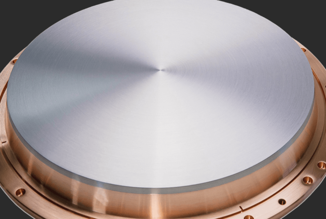
High purity targets, image source from the internet
1. High Purity Requirements
The primary characteristic of semiconductor high purity targets is their extremely high purity requirements. Purity levels are typically denoted by “n”, such as 5N (99.999%), 6N (99.9999%), 7N (99.99999%), etc. In semiconductor manufacturing, impurities in low purity targets can lead to increased film resistivity, thereby affecting chip performance. Especially in cutting-edge electronic manufacturing, high purity targets at the 7N level have increasingly stable performance, which is crucial for enhancing the performance of semiconductor devices.
2. Grain Refinement
In addition to high purity requirements, another significant characteristic of semiconductor high purity targets is their grain refinement. The smaller the grains, the more stable the physical and chemical properties of the target, which helps improve the material’s strength and toughness. This is important for preparing wear-resistant, corrosion-resistant, and optical functional coatings, with typical applications including tool coatings and decorative coatings. Grain refinement also helps reduce thermal stress during the sputtering process, minimizing cracking and peeling, thus improving sputtering efficiency and film quality.
3. Good Machinability
Semiconductor high purity targets must also possess good machinability to facilitate manufacturing and processing into various shapes and sizes. This includes mechanical processes such as cutting and polishing, as well as surface treatment techniques like chemical cleaning. Through precise mechanical processes and chemical cleaning, the surface flatness of the target can meet process standards, removing residual surface impurities and enhancing the target’s sputtering performance and film quality.
4. Strict Manufacturing Processes
The manufacturing of semiconductor high purity targets requires strict process control. From raw material purification to the final product, each step determines the product’s performance. The purification process employs a high vacuum environment to avoid introducing impurities from the environment or equipment. The powder preparation stage uses gas atomization or water atomization technology to produce uniform powders. The sintering and densification processes utilize cold isostatic pressing (CIP) and hot isostatic pressing (HIP) to eliminate porosity, enhancing the density and strength of the target. Vacuum melting and casting are used for the production of high purity metal targets. Homogenization annealing treatment can reduce internal stress and improve micro-uniformity.
5. Wide Application Fields
Due to their excellent performance, semiconductor high purity targets have a wide range of applications in semiconductor manufacturing, display manufacturing, solar cells, and more. In semiconductor manufacturing, targets are used to prepare thin film transistors, capacitors, resistors, and other components. In display manufacturing, targets are used to prepare conductive films and light-emitting layers in organic light-emitting diodes (OLED) and liquid crystal displays (LCD). In solar cells, targets are used to prepare electrodes and reflective layers in photovoltaic cells.
In summary, semiconductor high purity targets play an irreplaceable role in semiconductor manufacturing due to their high purity requirements, grain refinement, good machinability, and other characteristics. As semiconductor technology continues to develop, the performance requirements for targets will also become increasingly stringent. Therefore, strengthening the research and development and production of targets, improving their purity and stability, is of great significance for promoting the sustainable development of the semiconductor industry.
Welcome to join the semiconductor equipment and process communication group~Please add the editor and note your company+Name+Position. Note: This article is fromGlobal PNG (a B2B trading platform for semiconductors)The original link is https://www.global-png.com/information/detail/73, this article is only for disseminating semiconductor technology knowledge and not for other commercial purposes. Thanks to the original author. If there is any infringement or offense, please contact for deletion. Thank you~