
 Table of Contents1. RF Generator
1. Core Process of Energy Conversion
2. Engineering Significance of Key Indicators
3. Summary of Signal Chain Process
2. Impedance Matcher
1. Impedance Mismatch Issues and Matching Mechanisms
2. Comparison of Traditional Manual Matching and Automatic Matching Technologies
3. Automatic Matching Closed-Loop Workflow
4. Core Components of Automatic Matching Closed-Loop Control
5. Typical Failure Case: Handling Stuck Vacuum Capacitors
1. RF Generator
The RF generator, as the core energy supply device of the plasma system in semiconductor manufacturing, essentially achievesthe conversion of DC power to high-frequency AC power, providing stable energy to excite plasma for key processes such as etching, physical vapor deposition (PVD), and chemical vapor deposition (CVD).
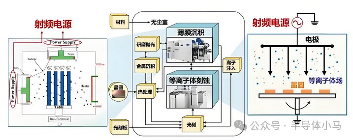
Its working principle can be summarized as follows: an oscillator generates a high-frequency oscillation signal (mainstream frequencies cover 400kHz, 2MHz, 13.56MHz, etc., with 13.56MHz products accounting for over 55% of the global market share), which is amplified to the target power level by a power amplifier, then filtered to remove harmonics and noise, and finally transmitted to the plasma reaction chamber through an impedance matching network (usually with a standard impedance of 50Ω) to achieve maximum power transfer.
1. Core Process of Energy Conversion
The energy conversion link of the RF generator follows the signal flow logic of Input-Processing-Output:
Input Stage:
Receives DC power (such as DC power from AC 220-240V after rectification) to provide basic energy for subsequent circuits.
Processing Stage:① Signal Generation: The oscillator generates a high-precision high-frequency signal, for example, the frequency accuracy of 13.56MHz can reach ±0.005%, ensuring the stability of the plasma excitation frequency (specific reference can be made to T-CPSS 1018-2025 Dynamic Impedance Testing Method for RF Power Supplies in Semiconductor Manufacturing);② Power Amplification: The signal power is increased to the process requirement range (from laboratory level 0-500W to production level 10kW) using Class D or H-bridge power amplifiers (efficiency over 90%);③ Signal Purification: Filters are used to suppress harmonics (usually < -50dBc), ensuring the purity of the output signal spectrum;④ Impedance Matching: The matching network dynamically adjusts the impedance to reduce reflected power (maximum reflected power usually ≤200W), achieving efficient energy transfer.Output Stage:The processed high-frequency AC signal is delivered to the reaction chamber, generating a high-frequency electric field to ionize the process gas, maintaining the concentration and uniformity of the plasma environment.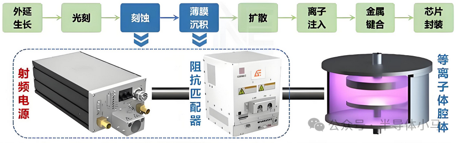
2. Engineering Significance of Key Indicators
The performance of the RF generator directly determines the yield of semiconductor processes, with core indicators including:
Frequency Accuracy: Must be controlled within ±0.005%; excessive frequency drift can lead to fluctuations in the thickness of the plasma sheath (the thickness of the sheath is inversely proportional to the frequency), which in turn affects the uniformity of ion energy distribution. For example, in dual-frequency capacitively coupled plasma (CCP), an increase in the frequency of the high-frequency source will reduce the sheath thickness and decrease the ion collision effect.
Power Stability: Must achieve an accuracy of ±0.1%-±1%; power fluctuations will directly change the plasma density and electron temperature, leading to deviations in etching rates or non-uniform film deposition thickness. For example, a 1% deviation in power stability may cause a film stress variation of over 0.5GPa.Industrial Standards: In semiconductor mass production equipment, RF generators must meet frequency accuracy ≤ ±0.005%, power stability ≤ ±0.1%, and response time <200ms to adapt to the rapid dynamic adjustment needs of plasma.
3. Summary of Signal Chain Process
The signal chain of the RF generator can be simplified as:
DC Input → Oscillator (Frequency Reference) → Power Amplifier (Power Amplification) → Filter (Noise Suppression) → Impedance Matching Network (Energy Matching) → High-Frequency AC Output (Plasma Excitation)
This process ensures the precise control of the “Energy-Plasma-Material” conversion in semiconductor processes through multi-level closed-loop control (frequency/power feedback), which is a key guarantee for improving the yield of advanced processes.
2. Impedance Matcher
1. Impedance Mismatch Issues and Matching Mechanisms
In RF power transmission systems, impedance mismatch is the core issue limiting energy transmission efficiency.
When the output impedance of the RF power supply (usually 50Ω) does not match the input impedance of the load (such as plasma reactors or antennas), part of the energy cannot be absorbed by the load, resulting in reflected power, which not only causes energy waste (up to over 40% of the input power) but may also lead to power supply overload, drift in chamber process parameters, or even damage to hardware.
For example, the impedance of plasma can dynamically change with gas type, pressure, power, and other process conditions. If matching is not timely, reflected power can instantly rise to hundreds of watts, directly affecting etching/deposition uniformity.
The impedance matcher achieves conjugate matching by adjusting variable reactance elements (capacitors/inductors), ensuring that the real part of the load impedance equals the source impedance, and the imaginary part is the opposite (i.e., when Z_source = R + jX, Z_load = R – jX). The core principle is to utilize the reactance characteristics of capacitors (X_C=1/(2πfC)) and inductors (X_L=2πfL) to construct L-type, π-type, or T-type matching networks, canceling the reactive components in the load impedance, making the total impedance consistent with the output impedance of the power supply.
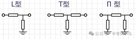
Taking the L-type network as an example, it consists of a tunable inductor (Q value >200) and a vacuum variable capacitor (50-1500pF). By dynamically adjusting the component parameters, it can achieve rapid impedance compensation in commonly used RF frequency bands such as 13.56MHz..
2. Comparison of Traditional Manual Matching and Automatic Matching Technologies
Manual matching relies on operators to manually adjust the capacitor/inductor knobs based on power meter readings, facing issues such as response lag (adjustment cycle usually >10 seconds), low accuracy (reflected power control error >5%), and poor repeatability, making it difficult to adapt to the rapid changes in plasma impedance in pulsed process scenarios.
Automatic matching technology achieves real-time dynamic adjustment of impedance through integrated sensors, control units, and actuators. A typical representative is Hanmin Technology’s three-capacitor structure matcher, whose core advantages include:
① Efficiency Improvement: Using real-time monitoring of the reflection coefficient (accuracy 0.01) and multi-range amplitude modulation strategies, matching efficiency is improved by 40% compared to traditional manual methods, especially suitable for scenarios with millisecond-level fluctuations in plasma impedance.
② Response Speed: Based on adaptive matching algorithms, tuning speed can reach 300ms per adjustment, quickly stabilizing power transmission during the plasma ignition phase (impedance change rate >10Ω/ms).③ Process Consistency: By storing optimal matching paths corresponding to different processes, preset parameters can be directly called during process startup, avoiding batch differences caused by manual adjustments.
3. Automatic Matching Closed-Loop Workflow
The automatic impedance matching system achieves dynamic balance through a closed-loop feedback mechanism of “reflected power → detection → adjustment → stabilization”, with the specific process as follows:
Reflected Power Monitoring: Real-time collection of voltage, current signals, and phase differences on the transmission line through a detection board (DETECTOR) and phase detection circuit, calculating the reflection coefficient (Γ) and voltage standing wave ratio (VSWR).
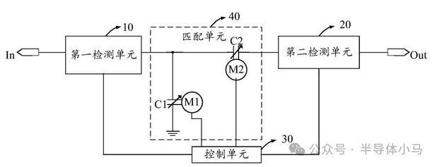
Signal Processing and Decision Making: The control unit calculates the target parameter values of adjustable components (capacitors/inductors) using least squares or genetic algorithms based on detection data. For example, when reflected power Pr > 5W, an adjustment command is triggered.
Execution Adjustment: The driving unit (stepper motor or servo motor) adjusts the variable capacitor (such as the position of the vacuum capacitor’s moving plate) and the number of turns of the inductor coil according to the control signal, changing the loop reactance value. The typical adjustable capacitor range is 50-1500pF, and the inductor tuning voltage range is -5V to +5V.
Stabilizing Output: Continuously monitor reflected power until Pr < 1%Pf (Pf is the incident power), and the system enters a steady state, at which point the impedance matching error is <0.5Ω.
4. Core Components of Automatic Matching Closed-Loop Control
Sensor Layer: Voltage/current probes (bandwidth ≥100MHz), AD8302 phase detectors (phase detection range -180° to +180°)
Control Layer: DSP processor (operating frequency ≥200MHz), adaptive matching algorithms (such as model predictive control)
Execution Layer: Vacuum capacitor drive motor (positioning accuracy ±0.01mm), inductor tuning mechanism (Q value maintained >200)
5. Typical Failure Case: Handling Stuck Vacuum Capacitors
During long-term operation, stuck vacuum capacitors are a common failure leading to matching failure, mainly manifested as abnormal sounds from the tuning motor and consistently high reflected power (>100W). The causes and handling solutions are as follows:
Failure Causes:
① Lack of lubrication in the moving plate bearing leading to mechanical jamming;
② Plasma arc discharge causing sintering on the surface of the moving plate (forming metal melt lumps)19.
Maintenance Process:
Disassembly and Inspection: Turn off the RF power supply, disassemble the matcher casing, and use a multimeter to measure the resistance between the capacitor poles. If the resistance is <10MΩ, it is determined to be an internal short circuit;
Ultrasonic Cleaning: Place the capacitor component in isopropanol solution and perform ultrasonic cleaning at 40kHz for 30 minutes to remove surface oil and sintering impurities;Lubrication and Assembly: Apply perfluoropolyether vacuum grease (temperature range -50℃ to 300℃) to the moving plate bearing, manually rotate the moving plate to ensure no jamming, and control the vacuum level <10⁻³Pa during assembly;Performance Verification: After installation, conduct no-load tuning tests to confirm that the capacitor adjustment range meets standards (50-1500pF), with reflected power <5W.
Through the above process, the capacitor’s service life can be extended to over 8000 hours, reducing equipment downtime by 30%.
Welcome to join the Semiconductor Equipment and Process Exchange Group~Please add the editor and note your company+Name+Position.
 Disclaimer: The content of this article comes from the public account (Semiconductor Pony). This article is only for organizing and promoting semiconductor industry knowledge, with no commercial purpose. Thanks to the original author. If there is any offense or infringement, please contact for deletion. Thank you~