What is SoC?
As the “brain” of fields such as smartphones, automotive electronics, artificial intelligence, and industrial control, SoC (System on Chip) is a highly integrated solution that combines computing cores, storage systems, communication interfaces, and various peripherals into a single chip.

The SoC architecture mainly includes four major components:1. Core CORE2. Memory MEM3. Peripheral Interface IO4. Bus BUS
Therefore, SoC typically includes one or more processing cores (such as MCU cores, CPU, GPU, DSP), storage units (such as RAM, ROM), communication interfaces (such as Wi-Fi, Bluetooth, Ethernet), peripheral interfaces (such as GPIO, ADC/DAC power), and other dedicated hardware modules. The goal of SoC is to embed a complete computing system into a single chip, thereby improving performance, reducing size, and lowering power consumption.
A typical SoC system-level chip structure includes the following parts:
·At least one microcontroller (MCU) or microprocessor (MPU) or digital signal processor (DSP), but can also have multiple processor cores;
·Memory can be one or more of RAM, ROM, EEPROM, and flash memory;
·Oscillators and phase-locked loop circuits for providing timing pulse signals;
·Peripherals consisting of counters and timers, power circuits;
·Wiring interfaces of different standards, such as USB, FireWire, Ethernet, universal asynchronous receiver-transmitter, and serial peripheral interfaces;
·ADC/DAC for converting between digital and analog signals;
·Voltage conditioning circuits and regulators.
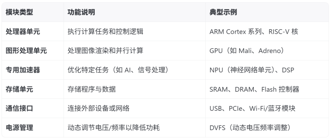
The computing core CORE is mainly divided into CPU, GPU, NPU, DSP:
CPU (Central Processing Unit)
ARM Cortex-A/R/M: Suitable for mobile devices, embedded devices, real-time computing.
RISC-V: Open-source architecture, suitable for self-developed chips.
GPU (Graphics Processing Unit)
Responsible for 3D rendering, game computation, AI acceleration (such as Mali, Adreno, PowerVR).
NPU (Neural Processing Unit)
Handles AI inference tasks, such as autonomous driving, smart cameras (Cambricon MLU, Huawei Ascend).
DSP (Digital Signal Processor)
Processes signal computations, such as audio processing (Qualcomm Hexagon).
SoC can be divided into edge SoC and server SoC based on application scenarios. Edge SoC is further divided into smart terminal SoC and IoT MCU SoC (or domain SoC). Application areas include mobile devices: smartphones (Qualcomm Snapdragon, Apple A series), tablets; IoT: smart home sensors, wearable devices; automotive electronics: in-vehicle entertainment systems, autonomous driving chips (such as Tesla HW4.0); embedded systems: industrial control, medical devices (such as heart rate monitors).
SoCs with built-in AI engine NPU are referred to as edge AI SoC chips. Among them, the core CORE is CPU, GPU for smart terminal AI SoC chips, and the core CORE is MCU for AIoT IoT terminal AI SoC chips, or called domain controller AI SoC chips.
The core CORE is a key component, and its type has a significant impact on overall performance. Currently, mainstream cores can be divided into three categories: CISC (Complex Instruction Set Computer), RISC (Reduced Instruction Set Computer), and RISC-V. CISC is represented by x86, widely used in PC and server fields; while RISC is represented by ARM, dominating in mobile chips and embedded systems.
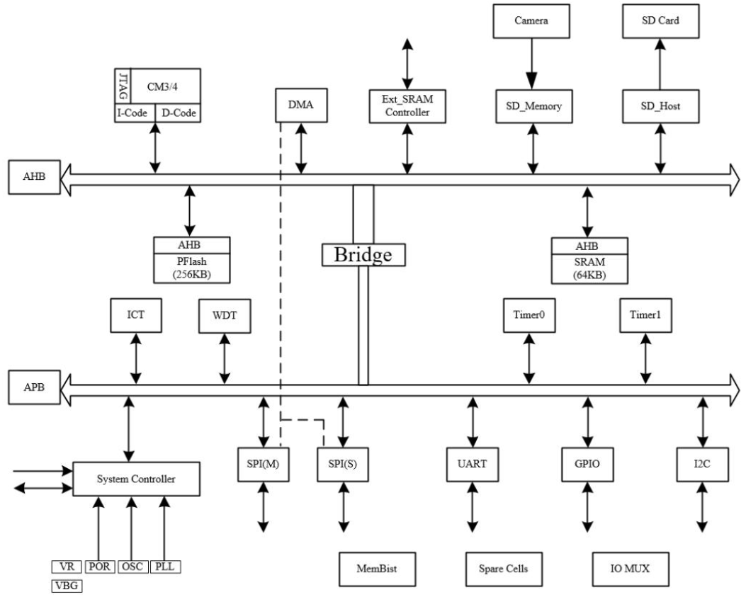
SoC core CORE generally includes three types of codes: I-Code represents instruction code, while D-Code represents data code. Additionally, JTAG technology is widely used in the chip debugging process to download and debug programs. I-Code and D-Code, namely I-Cache and D-Cache, are not used in every SoC, and their usage depends on the actual scale and specific needs of the chip.
For example, the code distribution mechanism of an ARM architecture chip is as follows:
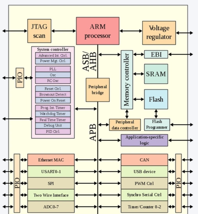
Different cores CORE can form different CPU, GPU, NPU. CPU refers to the serial instruction set algorithm core CORE, mainly responsible for workflow processing; GPU refers to the parallel instruction set algorithm core CORE, generally used for data compression and decompression processing, such as audio, video, text, and table processing; NPU refers to the neural network acceleration instruction algorithm core CORE, mainly running integral matrix algorithms. Chips with CPU+GPU together are called super chips, while NPU+CPU or GPU is called accelerated algorithm processing AISIC chips, which is equivalent to CPU+GPU+NPU AI artificial intelligence motherboard card.
SoC storage architecture includes the following parts:
Cache system: L1 (instruction/data cache), L2 (shared cache), L3 (on-chip cache).
External storage: DDR (LPDDR5X), eMMC/UFS (storage chips).
Storage unit MEM includes two types of memory: PFlash and SRAM. PFlash is similar to a hard disk, with the characteristic of retaining data without power loss. When PFlash storage space is insufficient, storage capacity can be increased by extending Flash, such as NFC (Nand Flash Controller). SRAM, as static random access memory, loses its data when power is off.
In contrast to SRAM is dynamic random access memory (DRAM), but SRAM retains data without refreshing, while DRAM needs to be constantly refreshed to maintain data. Due to the high density characteristics of DRAM, when a large amount of data needs to be stored, its composed Memory area is relatively small, thus it is commonly used in small SoCs. If SRAM storage space is insufficient, capacity can also be increased through Ext_SRAM.
After the system is powered on, the CPU reads instructions from PFlash, i.e., “software” code, to start the programs required for system operation. During the boot process, necessary codes are downloaded to SRAM for program execution. Therefore, critical programs such as BootLoader are usually stored in PFlash and will be automatically loaded into SRAM after power on, from which the CPU fetches instructions for execution. Since the storage rate of SRAM is higher than that of PFlash, programs are usually executed in SRAM, while boot programs and infrequently used data are stored in PFlash.
Other parts of the SoC system are called peripherals, which work in coordination with the core CORE and storage unit MEM through bus protocols. Peripheral IO is divided into two major categories: high-speed peripheral IO and low-speed peripheral IO. High-speed peripheral IO, such as DMA, Ext_SRAM Controller, SD_Memory, and SD_Host, operates at a frequency of AHB 100MHz, mainly handling high-speed data transfer and control tasks. Low-speed peripheral IO, including SPI, UART, GPIO, and I2C, operates at a frequency of APB 50MHz, more suitable for handling low-speed data and communication needs.
To efficiently handle larger volumes of data, SoC is also equipped with a DMA engine (Direct Memory Access), which has no external interface and connects directly to the CPU.
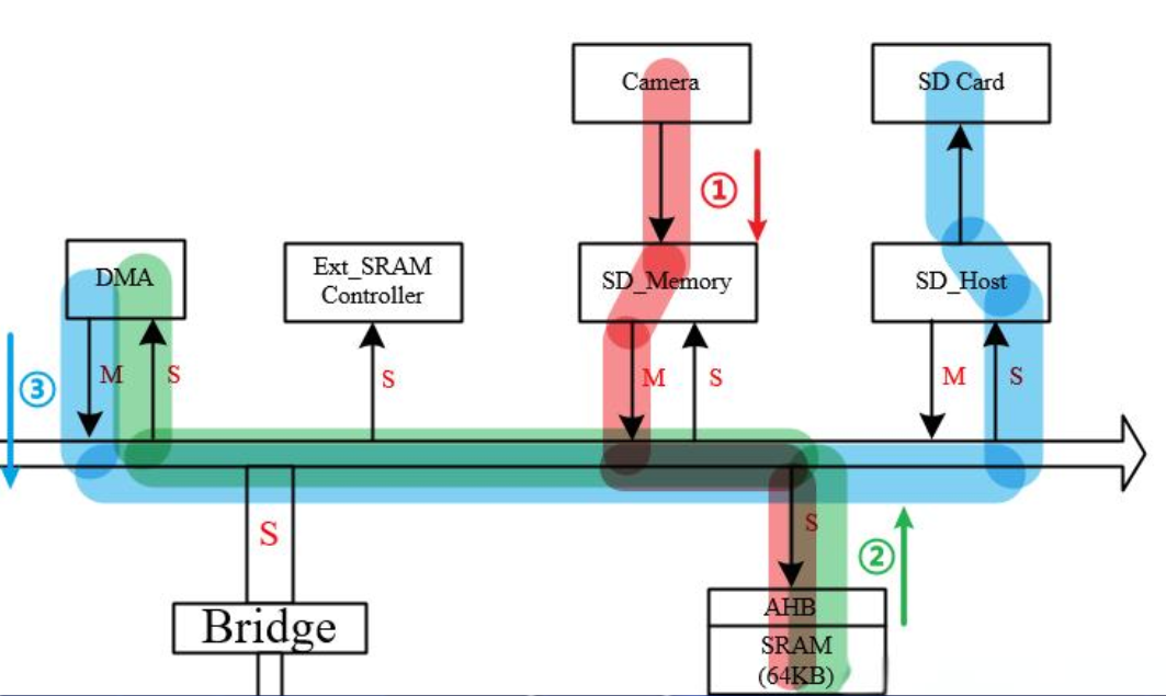
When the CPU needs to move a large amount of data from SRAM, the traditional approach is to first move the data to the CPU’s registers, and then transfer the data to the destination through instruction fetching and write operations. This method is not only inefficient but also occupies valuable processing time of the CPU. The DMA engine is designed to alleviate the CPU’s burden of moving data. The CPU only needs to inform the amount of data to be moved and the destination address, and the DMA will automatically perform the data transfer without continuous CPU involvement, only requiring the issuance of instructions.
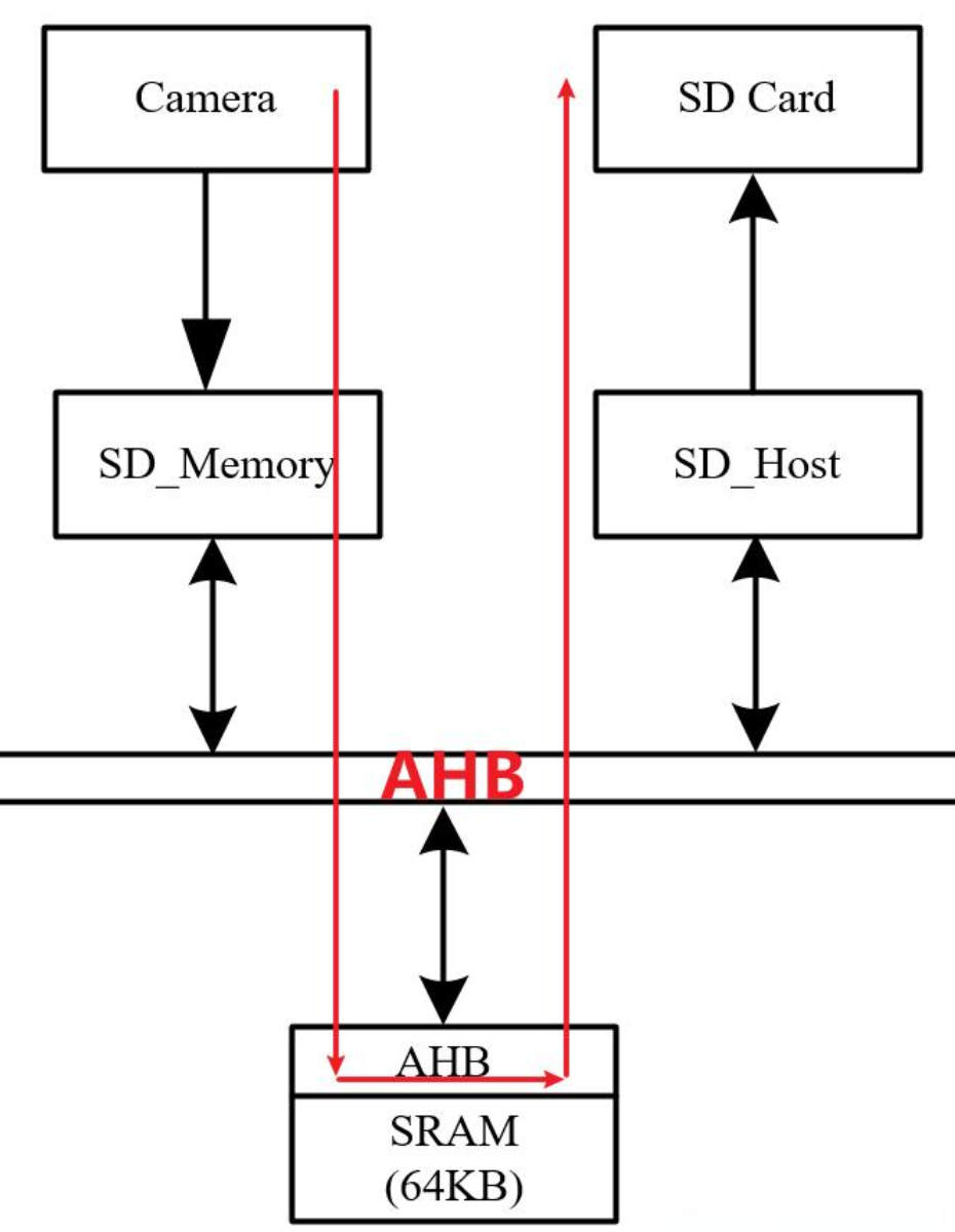
Additionally, SoC can also configure SD_Memory, usually connected to devices such as cameras and microphones, to store captured audio and video data through the SD_Memory interface into SRAM. Subsequently, the SD_Host interface further saves the data from SRAM to the SD card.
Common low-speed peripheral interfaces of SoC include I2C, UART, and SPI, each with its characteristics. The UART interface is commonly used for long-distance transmission but has a relatively low transmission rate, making it more suitable for point-to-point communication, where one interface can only connect to one UART Slave. The I2C interface has a faster transmission rate but usually does not exceed a specific limit, and I2C also supports connecting multiple Slave devices over short distances. The SPI interface is superior in speed compared to UART and I2C, and one SPI Master interface can connect to multiple SPI Slaves, but it requires more IO resources.
When peripherals communicate with the core CORE such as the CPU, two methods are typically used: one is the CPU actively querying the status of the peripherals; the other is the peripherals directly sending interrupts to the CPU, which processes them upon receipt. The BootLoader program and interrupt handling programs are pre-written and stored in FLASH, loaded into SRAM for use after the system starts. When an interrupt occurs, the system looks up and executes the corresponding interrupt handling program based on the interrupt vector number. In data transmission, the device that actively initiates data is called the master, while the device that passively receives data is called the slave.
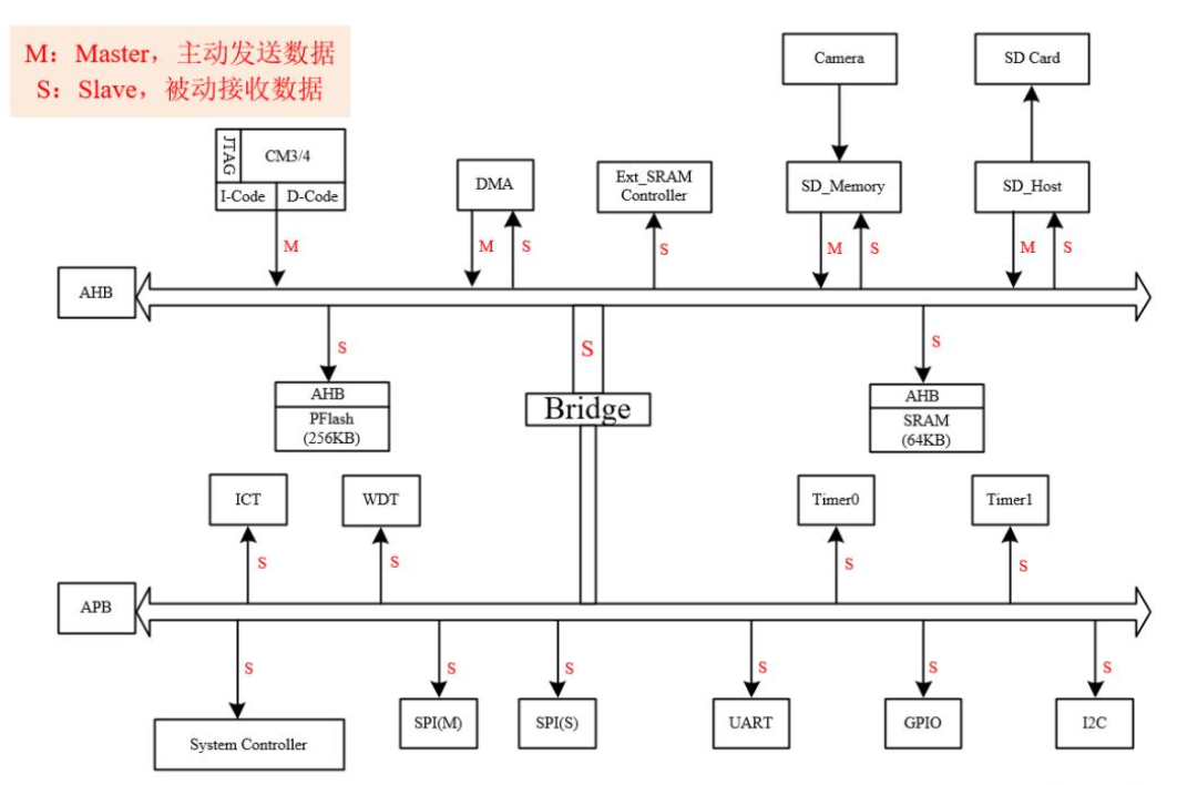
CPU usually plays the role of Master, as the initiator of data. Storage systems such as PFlash and SRAM exist as Slaves, passively receiving commands from the CPU and reading data from the corresponding addresses based on those commands. Additionally, the SD_Memory and SD_Host modules in AHB high-speed peripherals have dual functions as both Master and Slave: when the SD_Memory and SD_Host modules are working, data is transmitted through the Master port, while the Slave port is mainly used for CPU configuration.
Other slow peripherals such as SPI, UART, GPIO, I2C, Timer, WDT, and ICT interact with the CPU through the Slave port, where the CPU configures these peripherals to indicate the data that needs to be transmitted. This includes peripheral interfaces (USB, I2C, SPI, etc.) that allow communication with other devices.
External interfaces include the following parts: high-speed interfaces such as PCIe (connecting SSDs, expansion devices); USB 3.1/3.2 (data transmission); MIPI DSI/CSI (display and camera interfaces). Communication interfaces include Ethernet, Wi-Fi, 5G baseband (Qualcomm X70 5G baseband); UART, SPI, I²C, CAN (automotive and industrial control).
For example, the USB interface is used to connect external devices, I2C and SPI are used for communication with sensors and other low-speed devices, while UART is used for serial communication; network interfaces (Wi-Fi, Bluetooth, Ethernet) are typically integrated with wireless communication modules such as Wi-Fi and Bluetooth, as well as wired communication modules like Ethernet interfaces. These interfaces enable SoC to connect with other devices and networks in various applications such as IoT devices, smartphones, and tablets.
Additionally, SoC also contains some internal components, such as WDT (Watchdog Timer), a mechanism for monitoring system status. The core periodically “feeds the dog” to keep it active. If the core fails or hangs, the watchdog timer overflows and triggers an interrupt, notifying the external world that the chip has failed and needs to be addressed.
Timerx (hardware counter), a counter within the CPU, is used to measure time intervals. Typically, the CPU’s counting precision is low, only reaching microsecond levels, while our hardware counter can provide nanosecond-level precision. Additionally, using hardware counters can reduce the CPU’s burden and improve efficiency.
ICT (Instruction Count), a mechanism for counting instruction execution. It can track and record the number of instructions executed in a program, providing important data for performance analysis and optimization.
There are also other components, such as analog components including POR (Power On Reset), OSC (Oscillator), PLL (Phase Locked Loop), VBG (Voltage Management), and VR (Voltage Regulator), as well as small IO modules, all collectively referred to as IP (Intellectual Property). IP modules are typically pre-designed, reusable circuits or system components, such as processors, memory, interfaces, etc.
The internal communication bus (Bus/NOC) includes the following parts:
AXI/AHB/APB bus
AXI (high throughput, such as CPU ↔ DDR), AHB (high bandwidth, such as GPU), APB (low speed, such as UART).
NoC (Network-on-Chip) is suitable for multi-core SoC, improving communication efficiency (such as AI chips, autonomous driving chips).
Other collaborative management functional modules
In addition to interfaces, buses, and IP components, SoC has many other key modules. These modules work together to ensure that the SoC can efficiently perform various tasks. Key modules include but are not limited to clock management modules, power management modules, reset management modules, and debugging interface modules.
For example, MemBist technology mainly targets memory modules, especially SRAM, for built-in self-testing. During the chip manufacturing process, certain defects may be introduced, so after the chip is completed, a series of tests are conducted to ensure its quality. MemBist is an efficient built-in self-testing method. MemBist does not require external pins; it wraps a layer of Bist logic around the SRAM externally and triggers enable signals internally, allowing it to inject various test stimuli into SRAM and output processed stimuli, thus completing the built-in self-test of SRAM, which is the core function of MemBist.
Spare Cells are usually placed at the top layer of the chip, serving to quickly fix bugs discovered after chip production through ECO (Engineering Change Order, the process of manually modifying integrated circuits). During the ECO process, certain cells may need to be replaced, and the pre-placed Spare Cells can be directly used for replacement, thus avoiding the issue of insufficient die area that may arise from adding new cells, allowing for efficient repair work using Spare Cells without affecting the overall FloorPlan.
In after-sales repairs, for products with damaged cells, it is also possible to use the ECO method to mask the damaged cells and continue using them, but the functionality will be somewhat reduced due to the absence of some cells. This type of SoC is referred to as a ReMark chip in the industry. Sometimes, to make the functionality of the ReMark chip, which has fewer cells, similar to that of the original factory chip, some vendors may overclock the cells to enhance their functionality, but this may increase the chip’s power consumption and heat generation, and these products are colloquially referred to as “high-performance SoC chips” in the industry.
Pin interface management system
Additionally, SoC also includes a pin interface management system that connects to the outside world, such as the PAD pin allocation area, which is the specific area for connecting pins to the internal circuits of the chip; the Pin-MUX pin multiplexer, responsible for mapping a single physical pin to multiple logical functions, thus achieving flexible configuration of pin resources.
PAD includes three types: Input Only, Output Only, and Bidirectional. The Bidirectional type of PAD is the most commonly used, allowing flexible switching between input and output functions by controlling the EN signal. Additionally, some SoCs also have analog PADs, such as LVDS, and special types of PADs like VR (Voltage Regulator) PAD.
As an important interface for communication between the chip and the outside, PAD plays a key role in data transmission and exchange, while Pin-MUX effectively reduces the number of PADs. Through the collaboration of these two components, the SoC architecture can efficiently manage pin resources, providing greater flexibility and scalability for chip design.
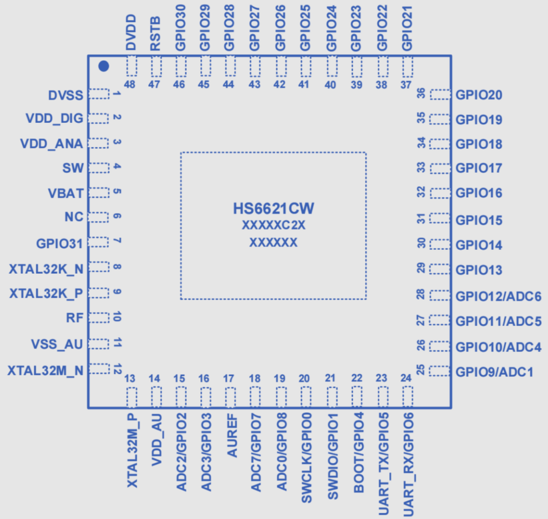
All of the above together constitute a complete SoC chip.
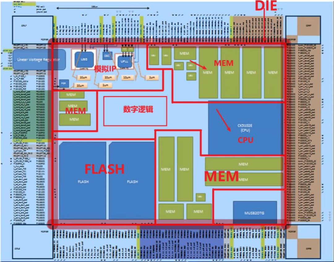
What IP components, communication protocols, and control ports are needed for SoC is mainly determined by chip design.SoC Design Process
A complete system-level chip consists of hardware and software, where software is used to control the hardware part’s microcontroller, microprocessor, or digital signal processor core, as well as external devices and interfaces. The design process of a system-level chip mainly involves the collaborative design of its hardware and software.
As the integration of system-level chips increases, design engineers must adopt reusable design ideas as much as possible. Most SoCs today use predefined IP cores (including soft cores, hard cores, and firm cores) to achieve rapid design through reusable design.
In software development, the protocol stack is an important concept used to drive industry-standard interfaces like USB. In hardware design, designers typically use EDA tools to connect pre-designed (or purchased) IP cores together in an integrated development environment (IDE) to integrate various sub-functional modules.
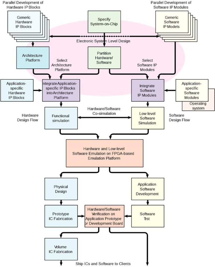
The design process of a system-level chip (Source: Wikipedia).
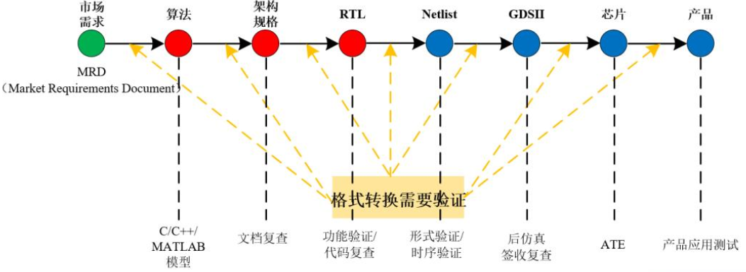
Before the chip design is sent to the wafer factory for production, designers will take different approaches to verify its logical functions. Simulation and verification are the most complex and time-consuming stages in the SoC design process, accounting for about 50% to 80% of the entire chip development cycle. Employing advanced design and simulation verification methods has become key to the success of SoC design.
MCU SoC is based on the MCU chip as the core CORE, adding bus protocols, and enhancing the core CORE, memory management system, by separating them from the audio and video management system, power management system, Bluetooth/Wi-Fi, and other communication protocol management systems, and integrating them together into a system on chip, mainly to compensate for the shortcomings of MCU computing power in data collection and transmission.
Among them, MCU (Microcontroller Unit), also known as a single-chip microcontroller, appropriately reduces the CPU’s main frequency and specifications, integrating various functional modules and interfaces such as memory, timers, A/D conversion, clocks, I/O ports, and serial communication into a single chip to achieve terminal control functions, with advantages of high performance, low power consumption, programmability, and high flexibility.
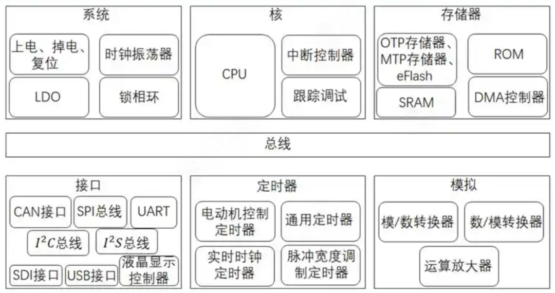
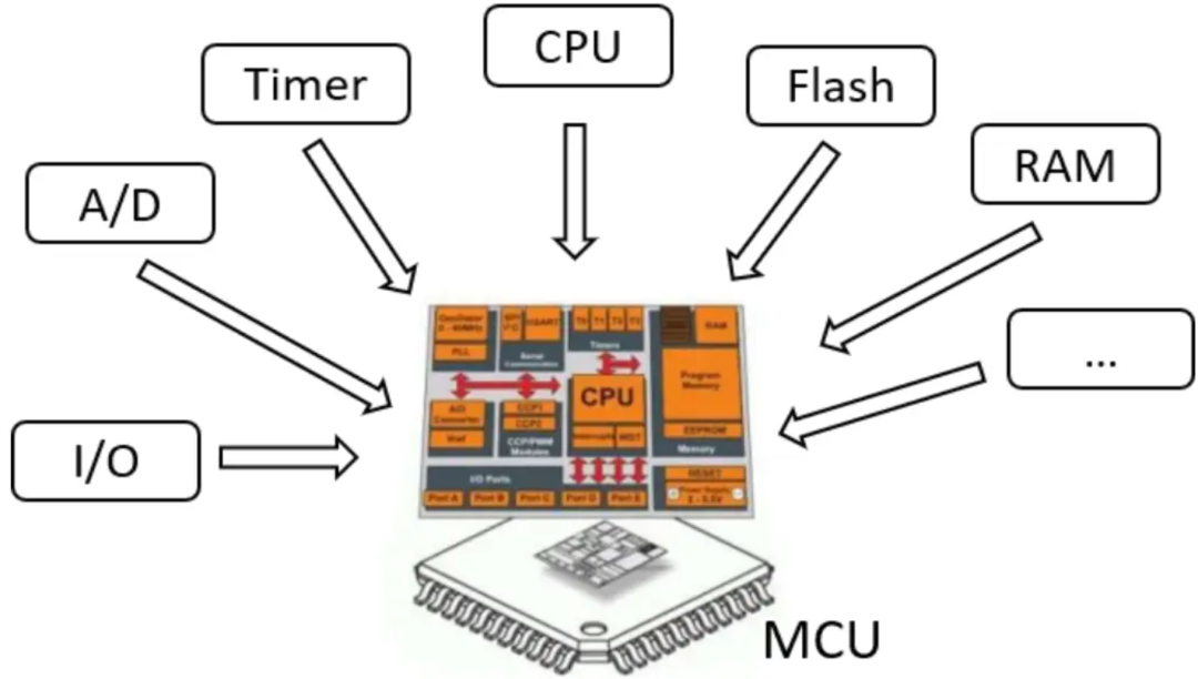
The internal composition of the simplest 51 core MCU includes CPU, RAM, ROM, timers (counters), serial ports, and external interrupts.
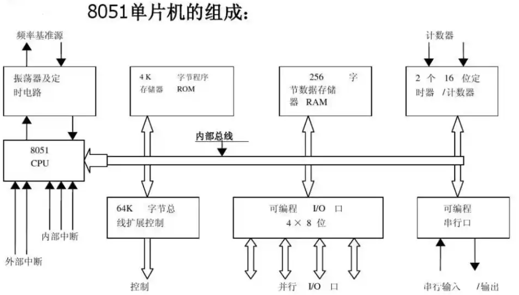
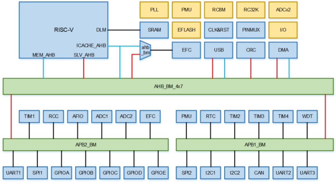
For example, the RISC-V architecture MCU mainly consists of the following parts.
For example, the internal composition of the ARMv7 architecture Cortex-M3 core STM32 is more complex.
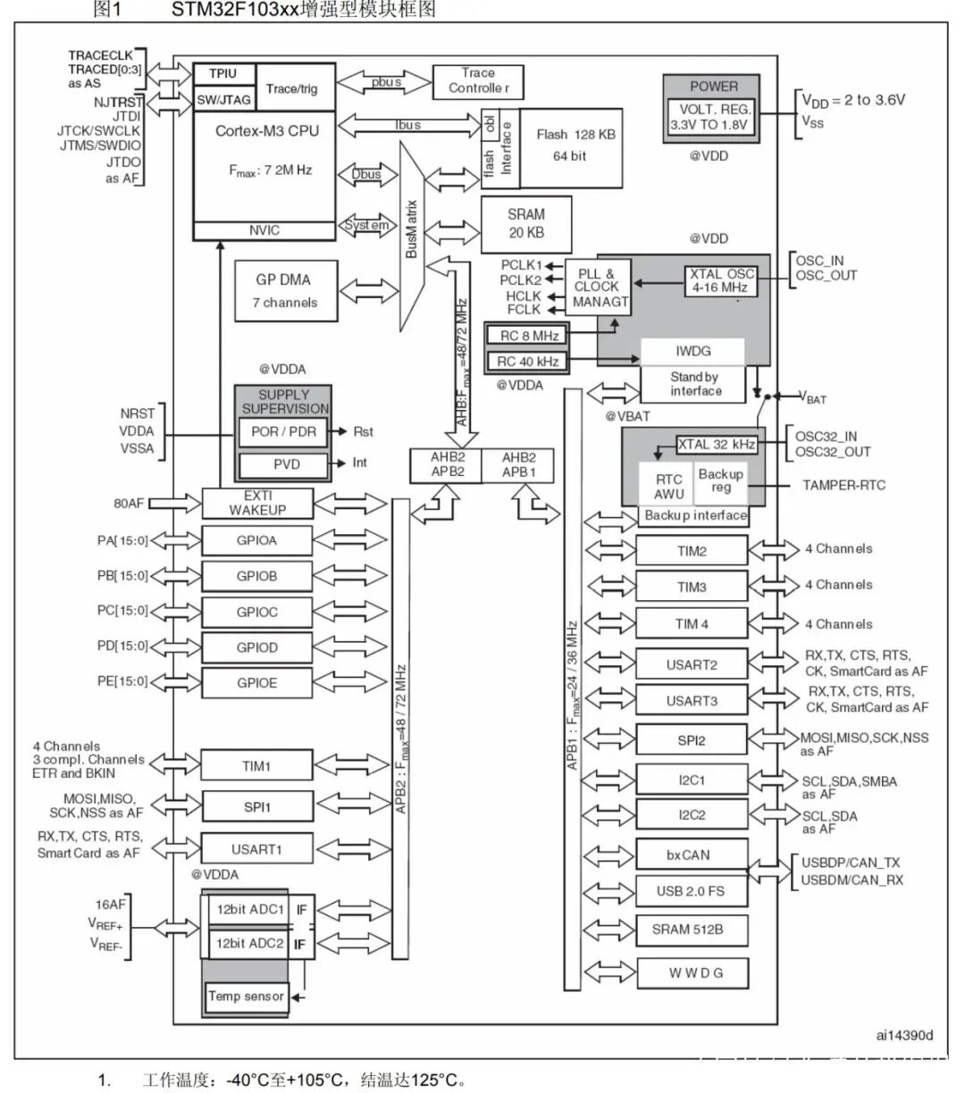
MCUs generally only run real-time operating systems (RTOS), mainly using “bare metal” programming.
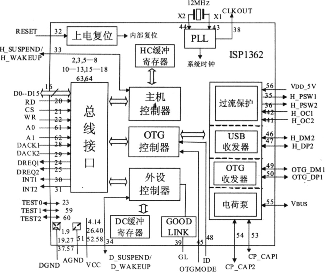
As data transmission capacity increases and bandwidth widens, many originally single functional modules belonging to MCUs and SoCs are also beginning to be designed as MCU units, including power management chips, RF communication chips, data transmission interface chips, etc., such as the USB 2.0 bus protocol interface chip below, which has three USB controllers: a host controller, device controller, and OTG controller:
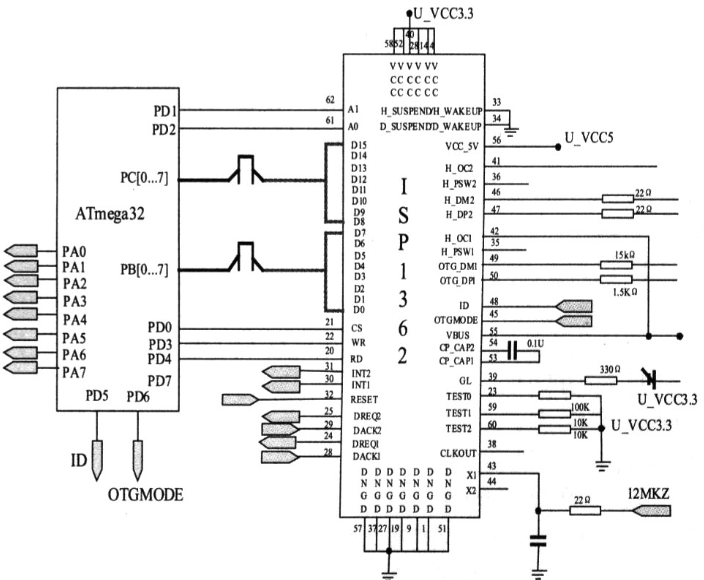
Additionally, there is a classification in the industry called MPU (Micro Processor Unit), also known as a microprocessor, which is a programmable special integrated circuit. MPU is just a processor and requires many other peripherals to form a system. In contrast, MCU has a processor, memory, Flash, and other modules integrated, requiring only a few peripherals to form a system.
MPUs were very popular in the 1980s, when microcomputers and game consoles used MPUs, such as Motorola’s 68000 chip, which was a mainstream microprocessor (MPU). The following is a circuit board of an Alpha Micro AM-1000 series microcomputer, with the largest chip in the middle on the right side being the MPU 68000.
Later, MPUs gradually declined, and it can be said that only Intel and AMD’s x86 series CPUs remain today. These CPUs are becoming increasingly complex, making it seem inappropriate to call them “microprocessors”. In the personal computer field, one can see motherboards like the one shown below. The motherboard, with CPU, memory modules, sound cards, etc., constitutes a computer. The entire motherboard is large and complex to manufacture.
The difference between MPU and MCU is that microcontrollers (MCUs) are often cheaper, simpler to set up, and easier to operate than microprocessors (MPUs). MCUs can be seen as single-chip computers, integrating ROM, RAM, etc., within the chip, while MPUs have peripheral chips that support various functions (such as memory, interfaces, and I/O) that can be replaced with different manufacturers’ peripherals. An important distinction between microcontrollers and microprocessors is that microprocessors typically run operating systems. Operating systems allow multiple processes to run simultaneously through multiple threads. Drivers are needed to support peripheral devices.
As the external functions integrated into MCUs increase, it has become increasingly difficult to determine whether a device is an MCU or an MPU. Because today, MCUs can perform many tasks, including more complex peripherals, the distinction between MCUs and MPUs has also become less clear. Now, some MCUs come with simple software drivers for more complex peripherals, resembling MPUs, and one can also find more MPUs with on-chip integrated peripherals that can perform MCU functions.
SoC is a system-level chip that can contain many MCUs, serving as a complete single-chip computer system capable of executing complex tasks with higher resource demands.
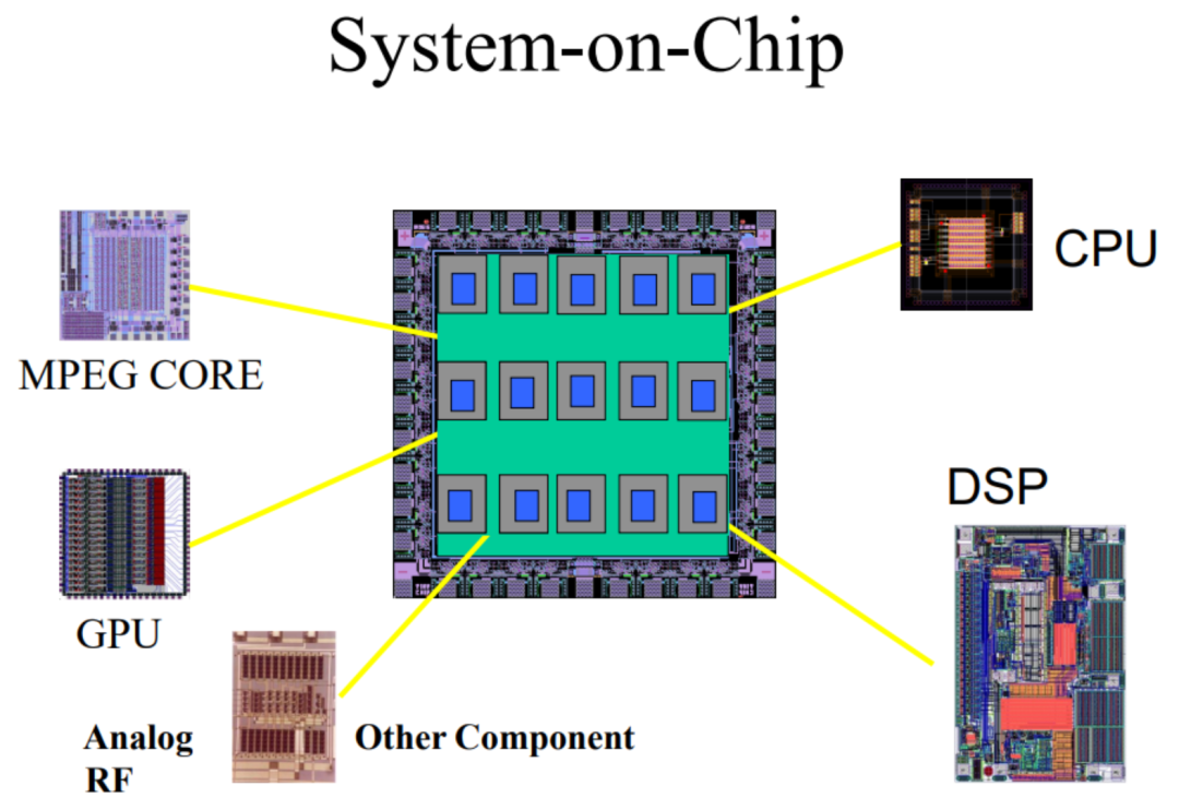
Low-end SOCs integrate MCU + specific functional module peripherals, which is the MCU SoC, while the MCU SoC integrated with NPU is called AI MCU SoC. High-end SoCs integrate MPU/CPU + specific functional module peripherals, which are commonly referred to as ordinary edge SoCs, server SoCs, AI SoCs, etc.
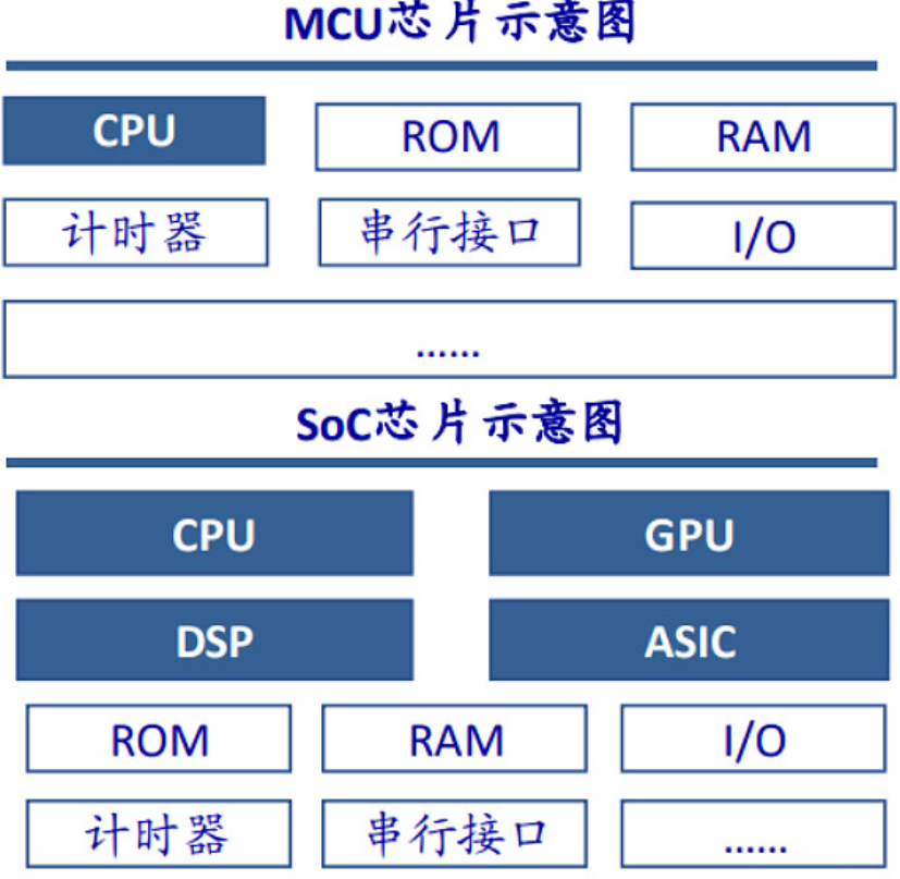
SoC refers to System on Chip, an overall circuit system that completes a specific function, indicating a system on chip, while MCU is a chip-level chip, and SoC is a system-level chip. It has the advantages of both MCU, which has built-in RAM and ROM, and MPU, which is powerful. It can not only run simple code but also system-level code, meaning it can run operating systems (mainly Linux OS) (considered a combination of MCU integration and MPU processing power advantages).
Additionally, there is SoPC (System On a Programmable Chip), which is not as frequently mentioned as the above concepts, but its importance is not diminished. SoPC stands for System On a Programmable Chip, which is a programmable system on chip. The most obvious difference between SoPC and MCU, MPU, SoC is that it allows for hardware configuration changes, meaning one can construct the chip themselves.
In simpler terms, the hardware configuration of an MCU microcontroller is fixed, and the programmable modifications are software configurations to select one or more functions; while SoPC can modify hardware configuration information to become the corresponding chip, which can be an MCU or a SoC.
As the NPU IP core matures, more and more sensors are beginning to integrate with DSP chips (digital signal processing chips), while also embedding NPU IP cores and other peripheral communication protocols, RF, etc., even upgrading the entire MCU functionality towards smart sensors; at the same time, some communication network card products are also beginning to integrate NPU IP cores and complete MCU cores, upgrading towards smart network cards; additionally, the power management chip industry is also developing its own NPU IP core to achieve on-demand peak shaving, achieving intelligent voltage regulation and current stabilization functions, meaning that most chips’ digital parts will initiate the development of feature code compression and decompression algorithms to achieve a combination of digitalization and intelligence, generating new AI chip architectures and products.
Basically, the route of computing power chips from simple to complex, and then to intelligent is: CPU, MPU, MCU, SoC, SoPC, AI DSP, AI SoC, and in the future, there may also be AI SoPC……