Photomask
/ PHOTOMASK
Did you know? The billions of fine circuits on a chip rely on a “micro film” to accurately “draw” them out — this is the photomask. From 193nm deep ultraviolet to 13.5nm extreme ultraviolet, from 28nm mass production to 14nm breakthroughs, this “small slice” of quartz and chromium film hides the core secrets of chip manufacturing and is crucial to China’s semiconductor localization battle. Today, we will dissect the “alchemy” of photomasks and see how they are reshaping the chip industry landscape!



01
Technical Analysis
How is a photomask “forged”?



PHOTOMASK
•

01
PART
First, understand: A photomask is the “micro film” of chip manufacturing>>>
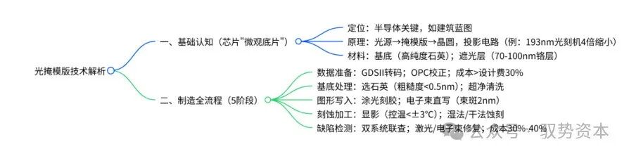
1.Positioning: In the semiconductor manufacturing field, photomasks are considered the key of keys, akin to the precise blueprints essential for constructing tall buildings. To put it another way, if chip manufacturing is likened to a super-precise micro “construction project”, then the photomask is the “construction blueprint”, without which the densely packed billions of circuits on the chip could not be accurately “drawn”.
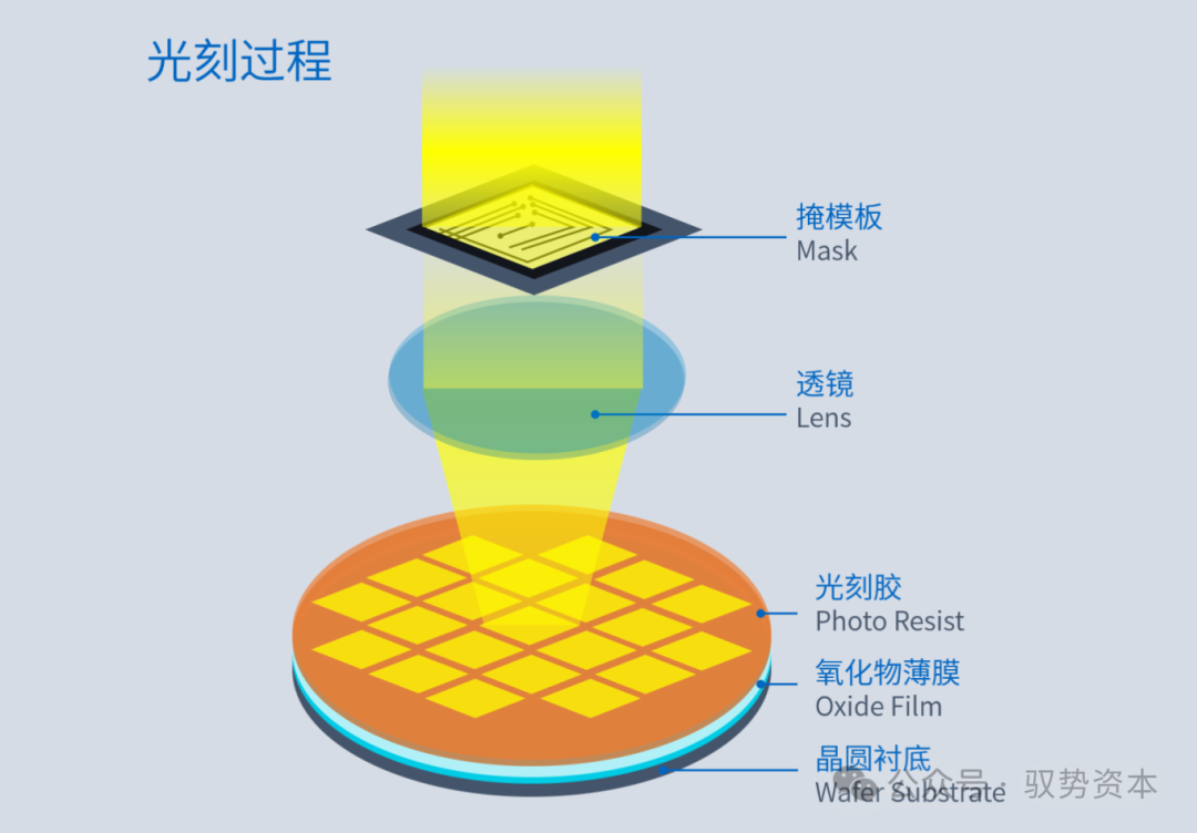
2.Working Principle (Analogy): If we imagine the photolithography process as a “light and shadow magic show” in the micro world, then the light source (such as deep ultraviolet light DUV or extreme ultraviolet light EUV) is the “spotlight” of this show, the photomask is a special “magic film”, and the wafer is the “photo paper” waiting to be “magically” transformed. When the light emitted from the light source passes through the photomask, the transparent areas on the photomask act like carefully designed “secret passages”, allowing the light carrying the circuit pattern information, like cheerful little sprites, to pass through these “passages” and be reduced and projected onto the surface of the photoresist-coated wafer, ultimately leaving precise circuit patterns on the wafer, completing this magical “light and shadow show”.
●For example, on the micro “big stage” of a 193nm immersion lithography machine, the originally 100nm lines on the photomask (which are already incredibly fine, much thinner than a human hair) will magically transform into ultra-fine line widths of only 25nm on the wafer after a 4x reduction, akin to shrinking a small pattern to a quarter of its original size in the micro world, with astonishing precision.
3. Material Black Technology:
● Substrate: The substrate material for photomasks is made of high-purity quartz glass, which is like an indestructible and super-transparent “crystal castle”. This material has astonishing properties, with a transmittance exceeding 99%, meaning that light can almost pass through it without obstruction. Additionally, its thermal expansion coefficient is extremely low, less than 0.5ppm/℃. This means that even if the surrounding temperature changes, even by 1℃, the dimensional change of the substrate is so small that it can be ignored. This outstanding stability is crucial for photomasks, ensuring that during the lithography process, the circuit patterns do not deform due to thermal expansion or contraction of the substrate, maintaining high precision at all times.
● Absorbing Layer: On the surface of the substrate, there is a chromium metal layer with a precisely controlled thickness of 70 – 100nm, which acts like a super powerful “light-blocking armor” for the “crystal castle”. Its light-blocking rate is extremely high, exceeding 99.9%, effectively blocking unwanted light and preventing light from leaking through areas it shouldn’t. Moreover, this “armor” cleverly avoids edge scattering effects, allowing light to maintain high precision when passing through the photomask, providing strong assurance for producing high-quality circuit patterns.


02
PART
Manufacturing Process: Harder than “Carving the Riverside Scene at Qingming on a Grain of Rice”>>>
The manufacturing process of photomasks is a super-precise “performance” in the micro world, meticulously divided into 5 stages, each with almost harsh precision requirements, with precision standards reaching nanometer level (to put it in perspective, 1 nanometer is merely 1/100,000th of a human hair’s diameter, so small it is almost unimaginable), making it as difficult as undertaking an “impossible task” in the micro world.
Stage 1: Data Preparation — “Pre-correcting” the Pattern
1.First Step: When chip designers use specialized EDA software to complete complex circuit designs, the next step is to convert this design file (usually in GDSII format) into a “language” that electron beam equipment can understand. This step is akin to drawing a detailed and precise “construction blueprint” for the subsequent manufacturing process; the electron beam equipment can only proceed with operations according to the design requirements if it understands this “blueprint”.
2.Key Operation: Optical Proximity Correction (OPC) is a super critical technology in the data preparation stage. In the micro world of lithography, the behavior of light is not as “obedient” as in the macro world; it exhibits diffraction effects, which means that light can “bend” during propagation. This characteristic can cause the originally designed circuit patterns to deform during the lithography process, like a well-done painting being blown off course by a mischievous wind. The OPC technology acts like a clever “graphic magician’s assistant”, preemptively applying “pre-distortion” processing to the circuit patterns through complex and sophisticated algorithms. In other words, it intentionally designs the patterns to appear “deformed” based on the diffraction laws of light, so that during the lithography process, after the light’s diffraction “interference”, the final pattern presented on the wafer can actually meet the initial design requirements.
●Taking TSMC’s 7nm process as an example, its design team needs to act like a group of tireless “micro explorers”, conducting thousands of simulations and repeated modifications to ensure the precision of the patterns. They must control the line width error within ±2nm on a micro scale; how precise is this? It’s equivalent to 1/35,000th of a human hair’s diameter, highlighting the strictness of this stage’s precision control.
3.Cost Warning: The design of advanced process chips is akin to a “money-burning battle”, with design costs often exceeding hundreds of millions of dollars, and this data preparation step accounts for over 30% of the total design cost. It can be said that this is a critical link in the chip manufacturing process that requires a significant initial investment, serving as an important foundation for the smooth progress of all subsequent work.
Stage 2: Substrate Processing — Grinding Quartz Glass to “Mirror Level”
1.Selecting the Substrate: Currently, the mainstream photomask substrates are made of 6×6 inch quartz glass, and the requirements for this “glass treasure” are extremely stringent, even more so than selecting a top-grade gemstone. Its surface roughness must be less than 0.5nm, while high-end products produced by Shin-Etsu Chemical in Japan can achieve an astonishing atomic-level flatness of 0.1nm. This requires the substrate’s surface to be as smooth as a super-smooth mirror, with no even the tiniest flaws; otherwise, when light passes through during the lithography process, it will encounter “roadblocks” and fail to complete its task accurately and precisely.
●In addition to surface roughness, the flatness deviation must also be less than 0.005%, ensuring that light maintains a stable propagation direction when passing through the substrate, without being “misaligned” due to substrate unevenness, which would affect lithography precision. The flatness of the substrate can be likened to a “highway” for light propagation in the micro world, which must be smooth and unobstructed to ensure the smooth progress of the lithography process.
2.Cleaning Process: After selecting the substrate, the next step is a super-fine cleaning “operation”. The cleaning process employs a combination of pure water ultrasound and active reagent soaking, akin to giving the substrate a comprehensive, deep “cleaning SPA”. The goal of this process is to remove all micron-sized dust particles from the substrate surface, with cleanliness requirements reaching less than 10 particles of >0.1 micron per cubic meter of air. What does this mean? The cleanliness of the photomask substrate is 100 times cleaner than that of a surgical room, highlighting the extreme pursuit of cleanliness; only in this way can the subsequent manufacturing process be free from any interference from impurities, ensuring the high-quality production of photomasks.
Stage 3: Pattern Writing — “Drawing” Nanopatterns with Electron Beams
1.Coating Photoresist: This step is akin to carefully “painting” a magical layer on the substrate. Using a spinning coater with a speed of up to 200,000 RPM, a layer of uniformly thick photoresist is coated onto the substrate surface with extreme precision, typically with a thickness between 0.5 – 1.5 microns, which is thinner than the plastic wrap we use in daily life. This layer of photoresist plays a crucial role in the subsequent pattern writing process, serving as a special canvas waiting to be adorned with exquisite patterns by micro “painters”.
2.Electron Beam Direct Write: Next, the electron beam direct write machine makes its appearance, acting like a super “painter” with a “magic pen” in the micro world. This device uses a 50 kV high-voltage electron beam as its “brush”, with a spot size of only 2nm, small enough to fit 5 atoms simultaneously, which is simply unimaginable. Moreover, its positioning accuracy is astonishing, less than 1nm, meaning it can accurately “draw” various nanometer-level patterns on the photoresist in the micro world.
●However, during this process, one detail needs special attention: the single-point dwell time must be controlled within 10 microseconds (1 microsecond is merely 1/1,000,000th of a second, an extremely short duration). This is because the electron beam generates heat during operation; if the dwell time is too long, it would be like continuously heating one spot, causing the photoresist to overheat and “burn”, leading to what is known as the thermal accumulation effect, which would severely affect the quality of the patterns. Therefore, it is essential to strictly control the single-point dwell time to ensure the precision and high quality of the pattern writing.
Stage 4: Etching Processing — “Carving” the Pattern onto the Chromium Layer
1.Development: The development process is akin to performing a special “fixing” operation on the patterns already “drawn” on the photoresist. Through standard development procedures, the exposed photoresist is removed, revealing the underlying chromium layer that needs to be etched. During this process, the temperature deviation must be strictly controlled to be <±3℃, as even slight temperature changes can affect the development effect, leading to pattern deformation or other quality issues, similar to adding different doses of catalysts in a chemical reaction. Therefore, the temperature during the development process must be precisely controlled, akin to managing an extremely precise chemical reaction, to ensure the accuracy of the patterns.
2.Etching Method: Choose One
● Wet Etching: Wet etching is like using a special “chemical knife” in the micro world. It employs chemical solutions (such as a mixture of hydrochloric acid and nitric acid) to dissolve the unwanted chromium layer slowly, akin to sculpting wood. This etching method is more suitable for processing micron-level patterns, akin to performing a fine “chemical carving” in the micro world.
● Dry Etching: Dry etching employs a more advanced technology — Reactive Ion Etching (RIE). It utilizes chlorine-based gases and chromium to create a “gas chemical reaction storm” in the micro world. During this process, chlorine gas interacts with chromium, converting the excess chromium layer into volatile products, which are then “blown away” like dust in the wind. For high-precision requirements such as 14nm processes, this dry etching technology must be used, as it can control line width errors within <±1nm and precisely set the sidewall angle to 85 – 90°, akin to constructing a steep cliff in the micro world, requiring the sidewalls to be very steep to ensure the precision and high quality of the patterns.
Stage 5: Defect Detection — “CT Scanning” the Photomask
1.Detection Tools: After completing the previous manufacturing steps, the photomask must undergo strict quality inspection, akin to performing a comprehensive “CT scan” on the photomask. The detection employs multiple magnification lenses combined with line scanning equipment, which act like super “microscope eyes”, capable of keenly identifying various defects larger than 20nm, such as pinholes and broken lines, which cannot escape their “keen eyes”. For high-end process photomasks, to ensure higher quality, a “dual-system joint inspection” method is also employed, using two different detection systems to conduct double checks on the photomask, ensuring that the defective dark spots are eliminated at a rate of over 99.9%, guaranteeing that every photomask leaving the factory is a high-quality product.
2.Repair Methods:
● Laser Repair: If defects are detected on the photomask, it is necessary to act like a “repair master” in the micro world and perform repairs. Laser repair technology is akin to using a magical “laser needle and thread” to precisely repair the defect areas by focusing the laser on them. This method is particularly suitable for addressing sub-micron line width errors and line end gaps, akin to performing a fine “surgical repair” in the micro world, restoring the photomask to its original state.
● Electron Beam Repair: Electron beam repair utilizes the electron beam as a “building material” in the micro world, filling in defects such as micro-holes by electron beam depositing metal. After the repair is completed, further detection is required to ensure that the light-blocking rate can be restored to >99.9%, ensuring that the performance of the photomask is not affected and meets high-quality standards.
3.Cost Proportion: In the production of high-end photomasks, the costs of detection and repair account for a significant portion of the total production cost, reaching 30% – 40%. This is akin to the inspection and maintenance costs in constructing a super luxurious building, highlighting the importance of these two stages in the photomask production process, serving as the final line of defense to ensure the quality of photomasks.

PHOTOMASK
•



02
Market Analysis
Global Landscape and China’s “Breakthrough Battle”


▋PHOTOMASK

Global Market: EUV Photomasks Become “Hotcakes”
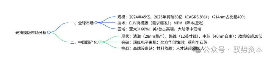
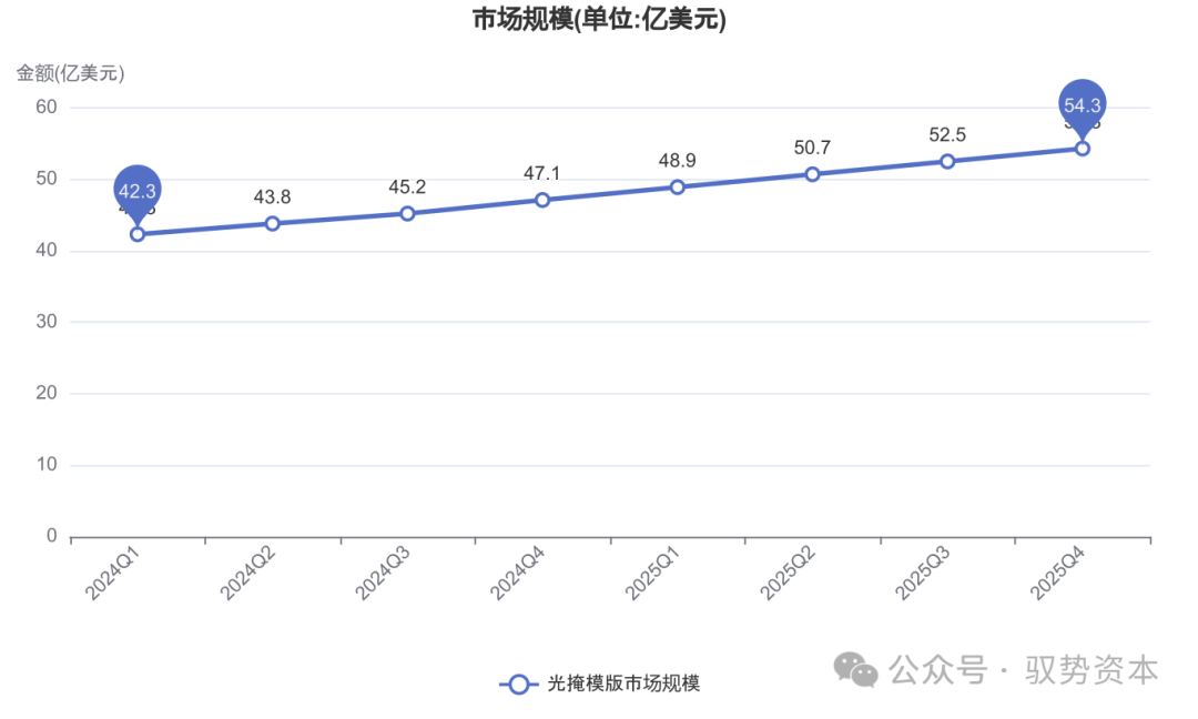
1. Scale: In the vibrant and competitive “big stage” of the global semiconductor market, the photomask market has shown a strong growth trend in recent years. By 2024, the global photomask market size is expected to reach $4.5 billion, resembling a “wealth balloon” that continues to expand, and this growth trend shows no signs of weakening. It is projected that by 2025, this “balloon” will continue to grow, with the market size surpassing $5 billion, achieving a compound annual growth rate (CAGR) of 6.8%. In this market, advanced process (≤14nm) photomasks are like the most dazzling “stars” on stage, accounting for over 40%, becoming the core driving force behind market development and leading the trend of the entire photomask market.
2. Technology Trends:
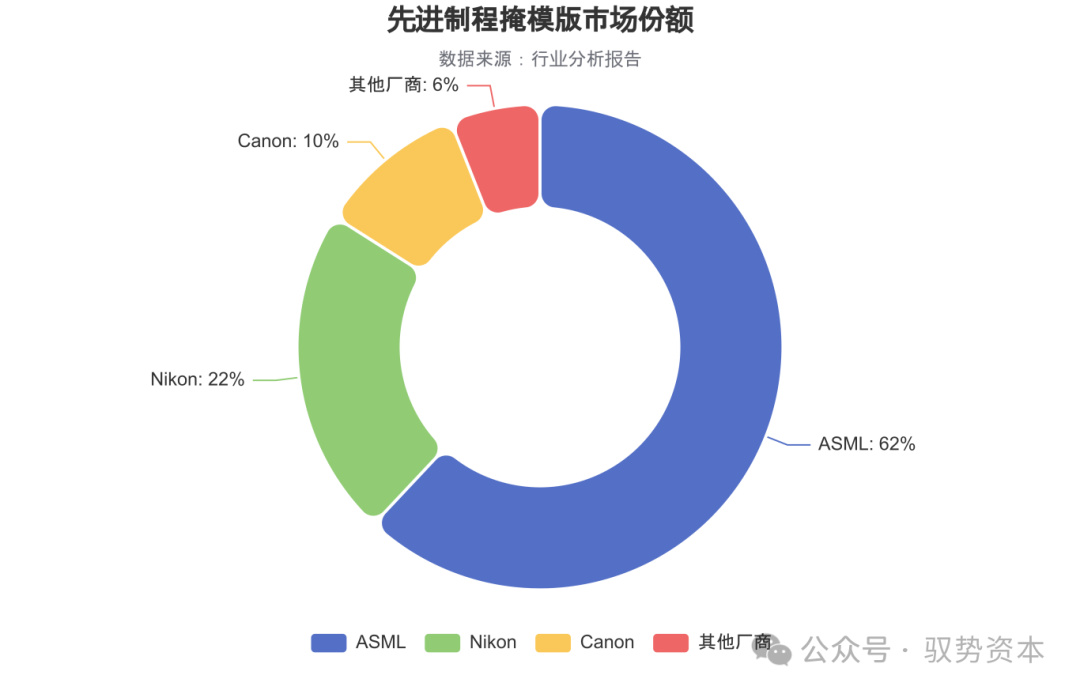
● EUV Photomasks: With the gradual popularization of extreme ultraviolet lithography technology (EUV), EUV photomasks have rapidly become “hotcakes” in the market, with demand showing explosive growth. This is because EUV lithography machines produced by companies like ASML have extremely high resolution, reaching 13nm, and to match this, the corresponding EUV photomask line width must be controlled within 3.25nm, posing unprecedented challenges to the manufacturing precision of photomasks and prompting related companies to continuously increase R&D investment, driving the rapid development of EUV photomask technology.
● Multi-Pattern Photomasks (MPM): Multi-pattern photomasks are like an “innovative darling” in the market. They have a unique advantage of transferring multiple layers of patterns in a single exposure, bringing an “efficiency revolution” to the chip manufacturing process. For instance, after adopting MPM technology in its 7nm process, Samsung significantly reduced the number of lithography steps by 30%, greatly improving production efficiency and significantly lowering manufacturing costs, giving chip manufacturers a competitive edge in the market, thus receiving widespread attention and application.
3. Regional Distribution: From a global regional distribution perspective, the Asia-Pacific region holds a crucial position in the photomask market, accounting for over 60%. Among them, China, South Korea, and Japan are the three major producing countries. Companies like Intel in the USA and TSMC in Taiwan are like the “dominators” of the high-end market, firmly holding a large share of the high-end market with their advanced technology and strong capabilities. Meanwhile, in the mid-to-low-end market, mainland Chinese companies are actively penetrating and gradually expanding their market territory, akin to brave “pioneers” striving to improve their market position in the competitive landscape.




03
Future Outlook
AI + EUV + 3D, Will Photomasks Change the Game?
PHOTOMASK
•
01
PART
Technological Integration: Three Key Directions>>>
(1) AI + Photomasks: Making “Drawing” Smarter
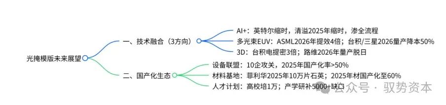
Traditional OPC optimization relies on manual adjustments by engineers, requiring 30 days for 7nm photomask design, which is prone to errors. The introduction of AI has completely changed this situation: Intel used AI OPC in its 10nm process, training models with millions of data points to autonomously optimize graphics, reducing design time to 15 days and improving yield by 5 percentage points; domestic company Qingyi Optoelectronics is collaborating with Huawei Cloud to develop a dedicated AI algorithm for 28nm, aiming to reduce design time from 20 days to 12 days and further increase yield by 3 percentage points after production in 2025. In the future, AI will also penetrate the entire process, such as predicting etching deviations and locating production line faults, driving photomask manufacturing towards “smart manufacturing”.
(2) Multi-Beam EUV Photomasks: Breakthroughs in Efficiency and Cost
Currently, EUV lithography machines use single-beam exposure, processing only 8 wafers per hour, leading to high costs. ASML plans to launch multi-beam EUV lithography machines in 2026, splitting into 16 sub-beams for simultaneous exposure, increasing efficiency by 4 times. The corresponding multi-beam photomasks need to integrate 16 identical patterns on the same substrate, with alignment errors <0.3nm, and must also incorporate anti-interference designs. TSMC and Samsung have already initiated R&D, with samples expected in 2025 and mass production in 2026, which will reduce unit costs by 50%, clearing cost barriers for 3nm and 2nm processes.
(3) 3D Photomasks: Adapting to Advanced Packaging
As terminal devices become lighter and thinner, chips increasingly require 3D integrated packaging (such as CoWoS and SiP). Traditional 2D photomasks require multiple exposures, leading to low efficiency and misalignment; 3D photomasks can transfer 3-5 layers of circuits in a single exposure through multi-layer pattern stacking. After using 3D photomasks for 5nm CoWoS packaging, TSMC increased interconnect density by 3 times and reduced packaging thickness by 40%; domestic company Luwei Optoelectronics is collaborating with Changjiang Electronics to develop a 2-layer 3D photomask, with mass production expected in 2026, aiming to eliminate dependence on Japanese companies.
02
PART
Domestic Ecosystem: Building “Our Own Circle” >>>
(1) Equipment Alliance: Joining Forces to Break the “Bottleneck”
Companies like Zhongwei and Northern Huachuang have formed an Equipment Alliance with 10 other companies to tackle challenges collaboratively: Zhongwei focuses on EUV etching equipment, Northern Huachuang is upgrading dry etching machines, and Suzhou Ruihong is optimizing electron beam direct write machines, aiming for a core equipment localization rate of over 50% by 2025. They have already received 1 billion in funding from the National Fund, and a complete set of domestic equipment solutions for 14nm photomasks is expected to be implemented by the end of the year.
(2) Material Base: Completing the Supply Chain
Hubei Feilihua is building a 12-inch quartz substrate industrial park, with a production capacity of 100,000 pieces per year by 2025, meeting 60% of domestic demand, with prices 40% lower than imports; the Jiangsu base is simultaneously advancing the development of 99.999% chromium target materials and 14nm photoresists, with mass production expected in 2025, increasing the localization rate of materials from 30% to 60%, mitigating supply chain risks.
(3) Talent Plan: Addressing the “Talent Shortage”
The Ministry of Education has included “Photomask Engineering” in the integrated circuit major, with 10 universities offering courses, aiming to train 10,000 talents over 5 years; Qingyi Optoelectronics is collaborating with Tsinghua University, and Luwei Optoelectronics is working with Wuhan University of Technology to conduct industry-university-research cooperation, focusing on training engineers and technicians to fill the gap of over 5,000 senior talents.
⦁⦁⦁
>> China’s “Light-Chasing Battle” for Photomasks <<
In 2025, China’s photomask industry will usher in a “breakthrough year” — 28nm mass production and 14nm awaiting production, but the gaps in high-end equipment, materials, and talent remain the “three mountains”. However, from breaking the quartz substrate monopoly to validating equipment in production lines, from policy support to ecosystem building, we have taken the crucial step of “from 0 to 1”.
In the future, seizing the opportunities of technological transformations in AI and multi-beam EUV, and completing the shortcomings of the industrial chain, China’s photomasks will ultimately shift from “catching up” to “running alongside”, becoming the most steadfast force in the “light-chasing battle” of the chip “micro world”.
–——-
Source: Official Media/Online News. Please delete if infringing.