In the process of circuit design, application engineers often overlook PCB layout. The common issues encountered are that the circuit schematic is correct, but it does not function properly or only operates at low performance… Have you faced this too? Today, I share an article by TI application engineer Timothy Claycomb on how to properly layout operational amplifier circuit boards to ensure their functionality, performance, and robustness, hoping to assist industry colleagues.
Taking the non-inverting configuration of the OPA191 operational amplifier as an example, designed with a gain of 2V/V, a load of 10kΩ, and a power supply voltage of ±15V. Figure 1 shows the schematic of this design.
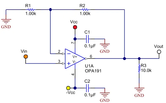
Figure 1: Schematic of the OPA191 in non-inverting configuration
The engineer assigned an intern to layout the PCB for this design and provided general guidance on PCB layout (i.e., minimizing the circuit board’s trace lengths while keeping components closely packed to reduce PCB space), then let him design independently. How difficult can the design process be? After all, it only involves a few resistors and capacitors, right?
Figure 2 shows his first attempt at the layout. The red lines represent the top layer paths of the PCB, while the blue lines represent the bottom layer paths.
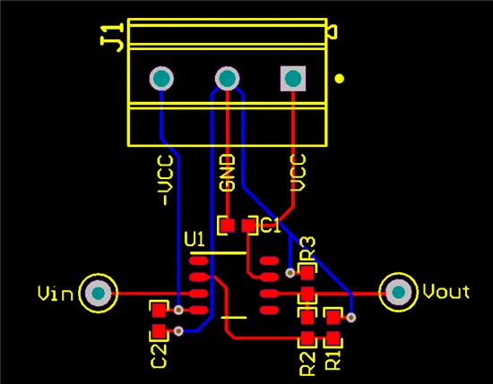
Figure 2: First layout attempt
At that time, the engineer realized that PCB layout is not as intuitive as I imagined; he should provide some more detailed guidance. He followed the recommendations strictly during the design, shortening the trace lengths and keeping the components closely packed together. However, this layout can still be further improved to reduce PCB parasitic impedance and optimize its performance.
The first improvement is to move resistors R1 and R2 next to the inverting pin of the OPA191 (pin 2); this helps to reduce stray capacitance at the inverting pin. The inverting pin of the operational amplifier is a high-impedance node, making it sensitive. Longer trace lengths can act as antennas, allowing high-frequency noise to couple into the signal chain. PCB capacitance at the inverting pin can cause stability issues. Therefore, the junctions at the inverting pin should be as small as possible.
By moving R1 and R2 next to pin 2, the load resistor R3 can be rotated 180 degrees, allowing the decoupling capacitor C1 to be closer to the positive power pin of the OPA191 (pin 7). It is extremely important to place the decoupling capacitor as close to the power pin as possible. If the trace length between the decoupling capacitor and the power pin is long, it will increase the inductance at the power pin, thereby degrading performance.
Another improvement made is regarding the second decoupling capacitor C2. The via connecting VCC with C2 should not be placed between the capacitor and the power pin, but rather positioned where the supply voltage must pass through the capacitor to reach the device’s power pin.
Figure 3 shows the method of moving each component and via to improve the layout.
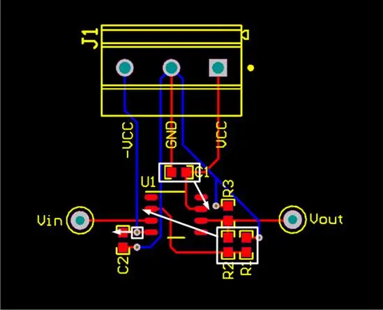
Figure 3: Positions of components after layout improvement
After moving the components to their new positions, further improvements can still be made. The trace widths can be increased to reduce inductance, which corresponds to the size of the pads connected to the traces. Additionally, a solid ground plane can be poured on the top and bottom layers of the PCB to create a solid low-impedance path for return currents.
Figure 4 shows the final layout.
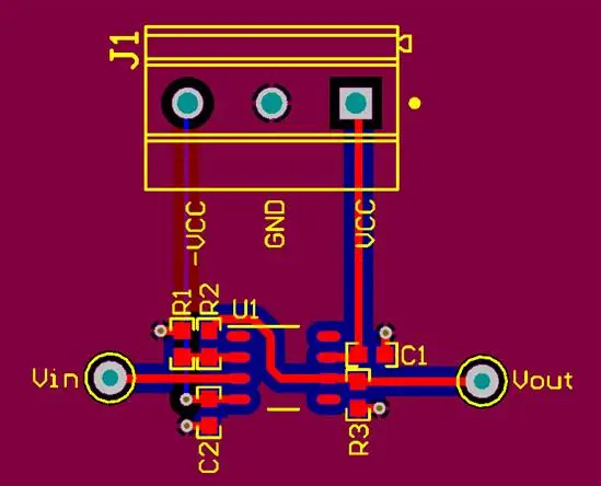
Figure 4: Final layout
The next time you layout a PCB, be sure to follow these layout practices:
-
Minimize the connections to the inverting pin as much as possible.
-
Place the decoupling capacitor as close to the power pin as possible.
-
If multiple decoupling capacitors are used, place the smallest decoupling capacitor closest to the power pin.
-
Do not place vias between the decoupling capacitor and the power pin.
-
Widen the trace paths as much as possible.
-
Avoid 90-degree angles in the trace paths.
-
Pour at least one solid ground plane.
-
Do not sacrifice good layout for the sake of silk-screening components.
Disclaimer: This article is copyrighted by the original author and does not represent the views of the association. The articles promoted by the “Jiangxi Province Electronic Circuit Industry Association” are for sharing purposes only and do not represent the position of this account. If there are copyright issues, please contact us for deletion.