Column Introduction
The design scheme of the Roewe RX5 MAX domain controller is a joint venture between SAIC and TTTech, called Chuangshi Smart Driving. The Roewe RX5 MAX is equipped with 3 millimeter wave radars, 6 full HD cameras, and 12 ultrasonic radars.
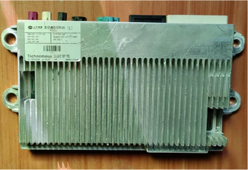
Front View of the Autonomous Driving Domain Controller Shell
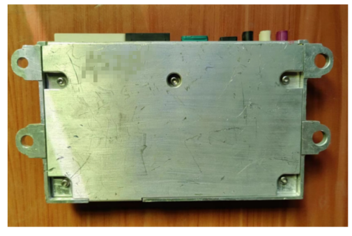
Back View of the Autonomous Driving Domain Controller Shell
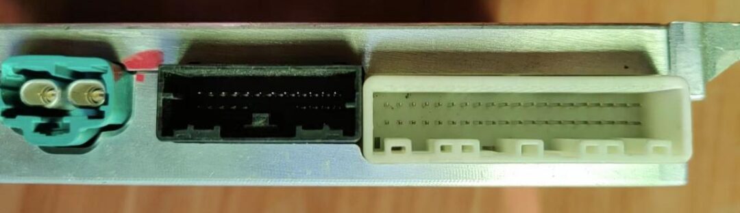
The above image shows the power, CAN, GPIO, and Gigabit Ethernet terminal interface of the Chuangshi Smart Driving Domain Controller
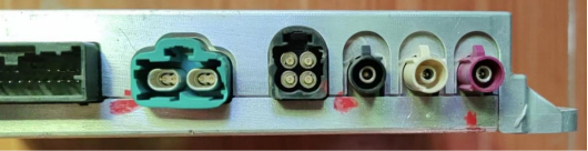
The above image shows the camera and antenna terminal of Chuangshi Smart Driving
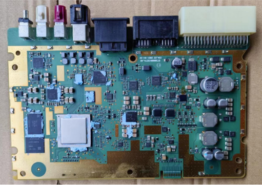
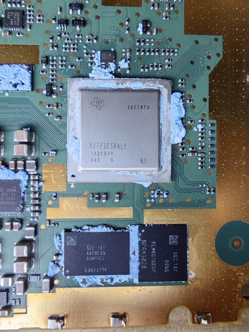
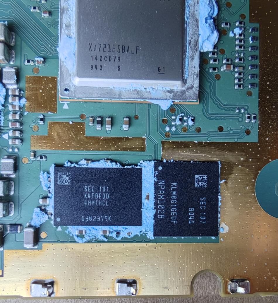
Front View of the PCB
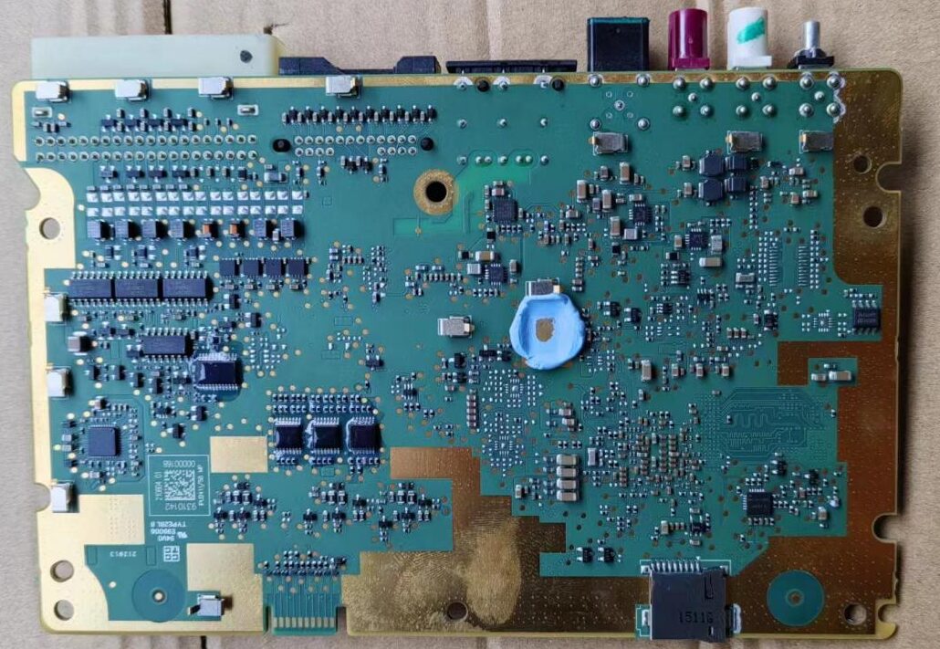
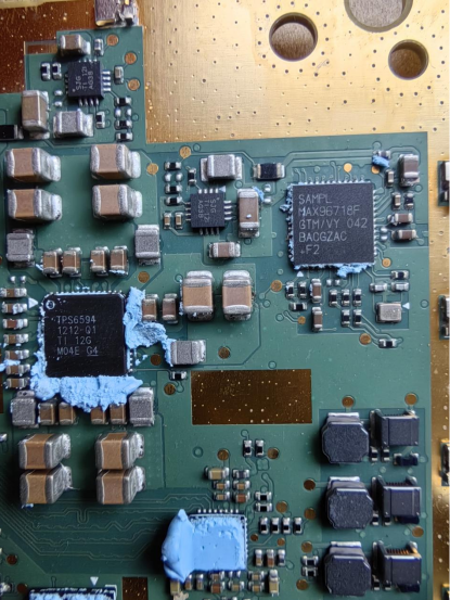
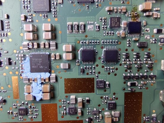
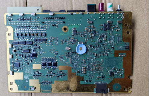
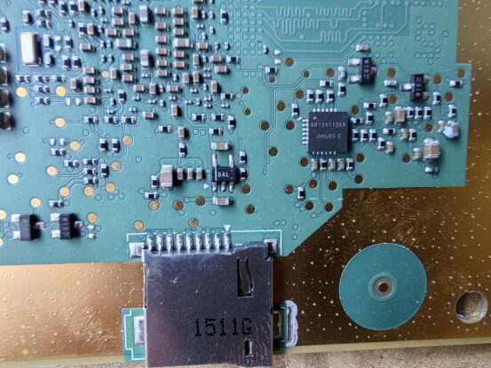
Back View of the PCB
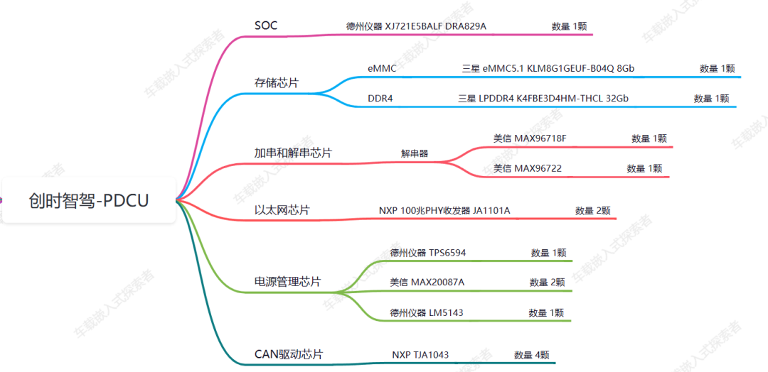
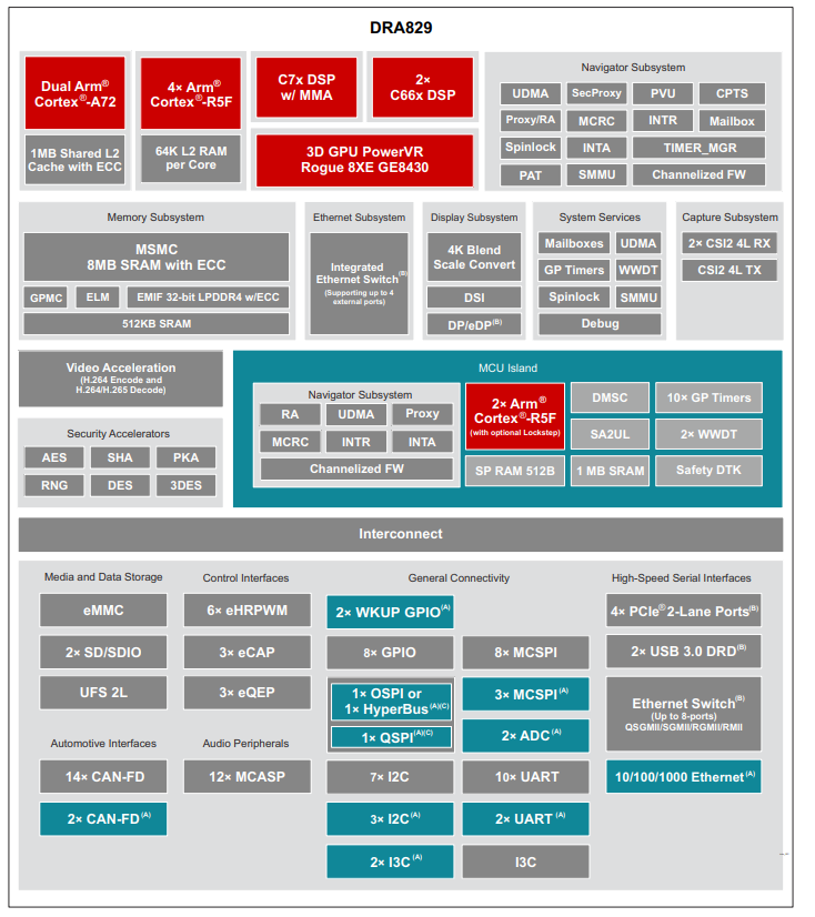
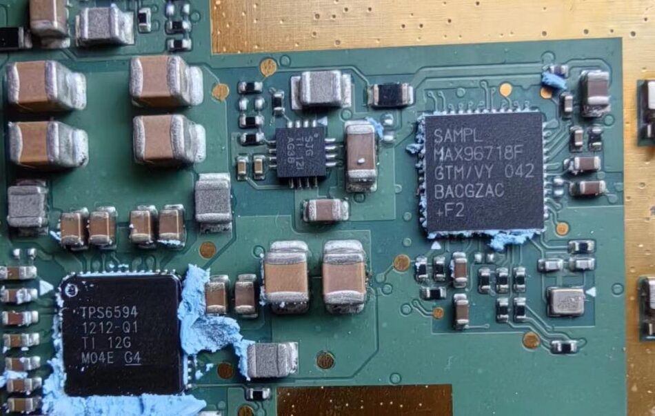
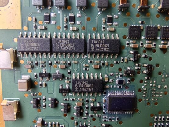
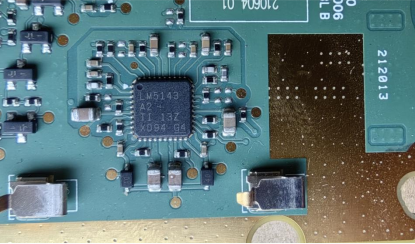
The Chuangshi Smart Driving Domain Controller uses a Texas Instruments DRA829 as the main control SOC, responsible for the implementation of perception, planning, and other algorithms; the storage chip consists of a Samsung EMMC chip and a DDR4 chip; the deserializer uses a Maxim MAX96718 and MAX96722; the Ethernet chip is NXP’s JA1101A; the power management chip is a Texas Instruments TPS6594, two Maxim MAX20087, and a Texas Instruments LM5143; the CAN bus driver chip is NXP’s TJA1043. Below, I will explain the characteristics and functions of each chip in detail.
4.1, SOC Chip
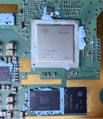
4.1.1, Introduction to DRV829
The DRV829 processor is based on the evolving Jacinto™ 7 architecture, aimed at ADAS and autonomous vehicle (AV) applications, built on TI’s extensive market knowledge accumulated over more than a decade in the ADAS processor market. In an architecture designed to meet functional safety standards, the unique combination of high-performance computing, deep learning engines, and dedicated signal and image processing accelerators makes the DRA829 device well-suited for various industrial applications such as robotics, machine vision, radar, etc. The DRA829 provides high-performance computing for traditional and deep learning algorithms with industry-leading power/ performance ratios, enabling scalability and lower costs for advanced automotive platforms supporting multiple sensor modes in centralized ECUs or standalone sensors. Key cores include next-generation DSPs with scalar and vector cores, dedicated deep learning and traditional algorithm accelerators, the latest Arm and GPU processors for general-purpose computing, integrated next-generation imaging subsystems (ISP), video codecs, Ethernet hubs, and isolated MCU islands. All of these are protected by automotive-grade safety hardware accelerators.
4.1.2, Role of DRA829 in Domain Controller
①, Perception Processing: The DRA829 enables real-time processing and fusion of multi-sensor data through integrated high-performance processors and digital signal processors (DSPs), used for target detection, target recognition, lane departure warning, pedestrian recognition, and other functions. It can process data from various sensors such as cameras, millimeter wave radars, ultrasonic sensors, etc.
②, Data Transmission and Storage: The DRA829 has high-speed data transmission and storage capabilities, supports multi-channel high-speed data interfaces such as Ethernet, USB, CAN, etc., for real-time reception and transmission of sensor data. In addition, the TDA4 supports high-capacity storage devices, allowing large amounts of on-board data to be stored for offline analysis and post-processing.
③, Decision-making and Planning: The DRA829 is equipped with a high-performance AI processor that can make real-time decisions and plans. It can predict and analyze the environment through deep learning models, generating safe and efficient path planning and dynamic decisions to achieve navigation and driving control of autonomous vehicles.
④, Safety Assurance: The DRA829 has multiple safety mechanisms, including hardware encryption, cellular communication security, and system integrity checks. It ensures secure transmission and storage of sensitive data, enhancing the safety performance of the autonomous driving system.
4.1.3, Features
|
Processor Cores: |
|
|
|
|
|
|
|
|
|
|
|
|
|
|
|
|
|
|
|
|
|
|
Block Diagram
4.2, Storage Chips
4.2.1, LPDDR4-K4FBE3D4HM
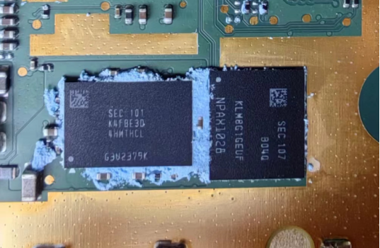
K4FBE3D4HM Introduction
Storage capacity: 32GB
Read and write speed: 4266 Mbps
Role:
①, LPDDR4 can provide fast storage access speed and high bandwidth, which autonomous driving systems need to perceive and analyze environmental data around the vehicle in real-time, including images, radar data, etc. The high-speed read and write capabilities of LPDDR4 can accelerate the data transfer speed between memory and processor, thereby improving system response speed and real-time performance.
②, LPDDR4 has low power consumption characteristics. Autonomous driving systems need to operate stably for long periods, often in embedded environments where heat dissipation and power consumption control are essential considerations. The low power design of LPDDR4 can reduce the controller’s energy consumption, extend battery life, and reduce heat issues, improving system stability and reliability.
③, LPDDR4 supports high-density storage and large-capacity memory, and autonomous driving systems need to store and manage a large amount of map data, vehicle status data, historical control information, etc. The high-density storage capability of LPDDR4 can meet these needs while ensuring high-speed read and write and processing performance.
Features
|
• Dual data rate architecture; two data transfers per clock cycle • Bidirectional data strobe (DQS_t, DQS_c), sent/received together with the data used by the receiver when capturing data • Differential clock input (CK_t and CK_c) • Differential data strobe (DQS_t and DQS_c) • Commands and addresses on the positive CK edge; the two edges of DQS reference the data and data mask • Each mold consists of 2 channels • Each channel has 8 internal banks • DMI pin: DBI (Data Bus Inversion) during normal write and read operations, used for masking write data (DM) when DBI is off -Count # of masked written DQ 1 when DBI is on • Burst length: 16, 32 (OTF) • Burst type: continuous • Read and write latency: see table 64 LPDDR4 AC timing table • Automatic precharge option for each burst access • Configurable drive strength • Refresh and self-refresh modes • Partial array self-refresh and temperature-compensated self-refresh • Write leveling • CA calibration • Internal VREF and VREF training • FIFO-based write/read training • MPC (Multipurpose Command) • LVSTL (Low Voltage Swing Termination Logic) IO • VDD1/VDD2/VDDQ: 1.8V/1.1V/1.1V • VSSQ terminal • No DLL: CK to DQS unsynchronized • Edge-aligned data output, data input center-aligned write training • Refresh rate: 3.9us |
4.2.2, eMMC KLM8G1GETF
KLM8G1GETF-B041 Introduction
Storage capacity: 64GB
Role:
①, This eMMC chip is one of the main media used to store the firmware and operating system of the controller. The firmware and operating system of the main controller are burned into the eMMC chip to be loaded from the chip at startup. This ensures system stability and consistency, allowing the controller to boot quickly.
②, The eMMC chip is also responsible for storing and managing the running code in the controller. Autonomous driving controllers need to process a large amount of data and complex algorithms, and the running programs require high real-time performance and efficiency. The eMMC chip provides fast data read and write speeds, effectively executing the running code of the controller and ensuring its normal operation.
③, The eMMC chip is also used to store and manage data in the controller. Autonomous driving systems need to record and store various sensor data, map data, and other important data in real-time to support real-time decision-making and improve algorithms. The eMMC chip provides large storage space and high-speed data read and write capabilities, meeting the data storage requirements of autonomous driving controllers.
4.3, Serializer/Deserializer Chips
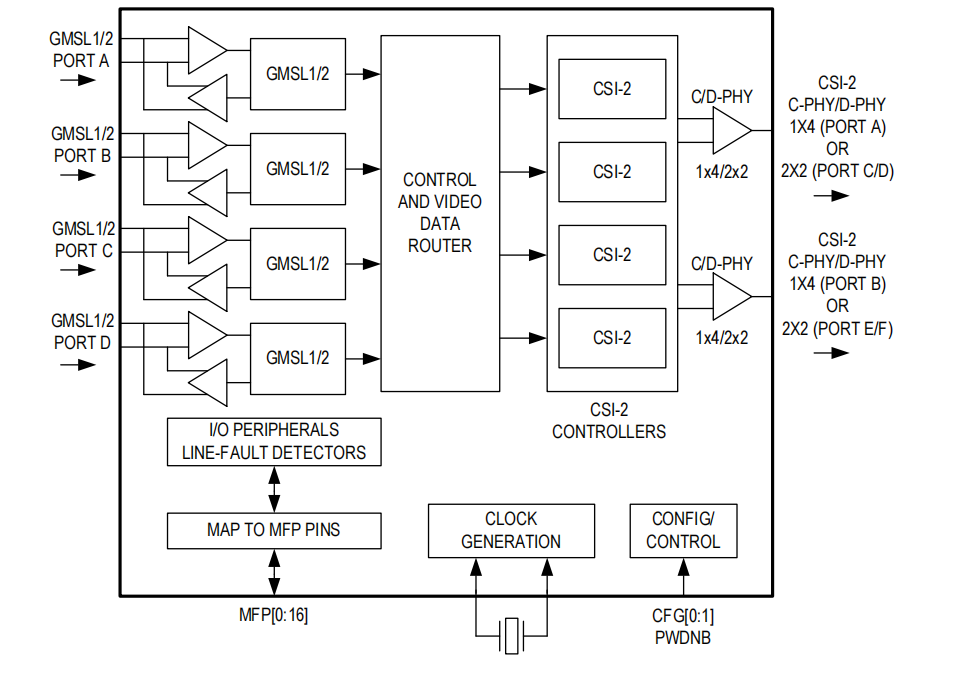
4.3.1, Maxim MAX96722
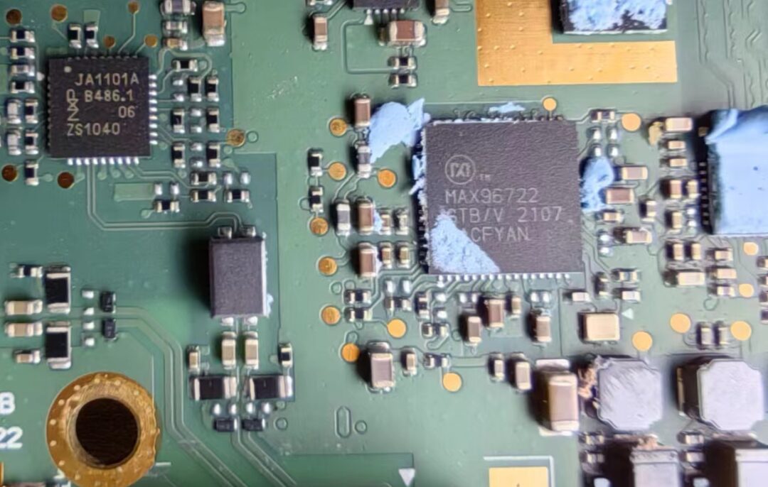
Introduction
The MAX96722 deserializer converts GMSL2 or GMSL1 serial input to MIPI CSI-2 D-PHY or C-PHY format output. This device allows each link to transmit bidirectional control channel data simultaneously during forward video transmission. The MAX96722 can accommodate up to four remote sensors using industry-standard coaxial cables or STP interconnects. Each GMSL2 serial link operates at a fixed rate of 3Gbps in the forward direction and 187.5Mbps in the reverse direction. In GMSL1 mode, the MAX96722 can pair with first-generation 3.12Gbps or 1.5Gbps GMSL1 serializers or operate in GMSL1 with GMSL2 serializers up to 3.12Gbps.
The MAX96722 supports video data aggregation and replication, allowing streams from multiple remote sensors to be combined and routed to one or more available CSI-2 outputs. Data can also be routed based on virtual channel IDs, allowing multiple streams from a single GMSL input to be routed independently to different CSI-2 outputs. Alternatively, frame-level cascading can be used to synchronize and combine data from multiple sensors into a single CSI-2 stream within a composite superframe. The CSI-2 interface supports 2×4 channel and 4×2 channel configurations using C-PHY or D-PHY.
Features
|
MIPI CSI-2 v1.3 output configurable as 2×4 channels, 1×4 lane + 2×2 lane, or 4×2 lanes |
• Optional D-PHY v1.2, 80Mbps-2.5Gbps/Lane or C-PHY v1.0, 182Mbps-5.7Gbps-Lane • 16/32 channel virtual channel support (D/C-PHY) • Flexible aggregation and routing of incoming data via CSI-2 VC or frame-level cascading • Data can be replicated and routed to any CSI port • Supports RAW8/10/12/16/20, RGB565/666/888, YUV422 8-/10-bit formats • Dual pixel mode enhances transmission efficiency • CSI-2 lane reassignment and polarity inversion • MIPI/GMSL video PRBS generator and checker • Checkerboard/color gradient pattern generator • Raw CSI-2 PRBS generator • Independently configurable video paths and GMSL/CSI-2 ports |
|
Independently configurable four-way GMSL input GMSL1/2 operation, link speed, and video format |
• Mixed GMSL1/GMSL2 support • Backward compatible with GMSL1 serializers • GMSL1 forward link speed up to 3.12Gbps • 3Gbps GMSL2 link speed (forward) and 187.5Mbps (reverse) • Synchronization and simultaneous support for asynchronous cameras • Achieve precise synchronization for large camera systems’ serializers • GMSL PRBS generator/checker for link testing • Eye monitor for continuous diagnostics • Adaptive equalization for coaxial cables up to 15 meters • Compatible with 50Ω coaxial cables or 100Ω STP |
|
Compatible with ASIL-B (GMSL2) |
• Video watermark insertion and detection • 16-bit CRC protection for control channel data Retransmission upon error detection • Optional 32-bit CRC protection for video line data • ECC protection for video data memory • CRC protection for CSI-2 data streams |
|
Concurrent control channels for device configuration and communication with remote peripherals |
• 3 I2C/UART, 2 SPI, 17 GPIO • Eight hardware selectable device addresses |
|
Programmable spread spectrum to reduce EMI |
|
|
Line fault monitoring for GMSL links |
|
|
64-pin 9 x 9mm TQFN with exposed pads |
4.3.2, Maxim MAX96718
Similar performance to MAX96722, detailed chip manual not found!
4.4, Ethernet/Switch Chip
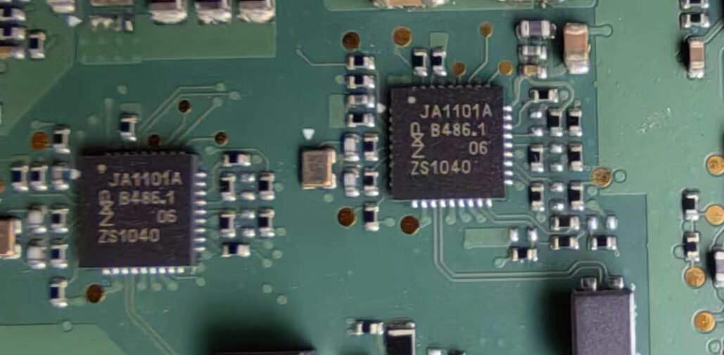
Introduction to TJA1101
The TJA1101 is an Ethernet PHY compliant with the 100BASE-T1 standard, optimized for automotive use cases such as gateways, IP camera links, driver assistance systems, and backbone networks. This device provides 100Mbit/s transmission and reception capability over two unshielded twisted pairs, supporting cable lengths of at least 15m.
The TJA1101 is designed for automotive robustness and ISO 26262, ASIL A compliance, while minimizing power consumption and system costs. Due to ASIL-A compliance, adequate safety features have been implemented to ensure that ASIL requirements are met at the system level.
Features
|
Function Overview |
Features |
|
General |
• 100BASE-T1 PHY • MII and RMII compatible interfaces for the bus • Compact HVQFN 36-pin package (6×6 mm) suitable for PCB space-constrained applications • ISO 26262, compliant with ASIL-A |
|
Optimized for Automotive Use Cases |
• Optimized transmitter for capacitive coupling with unshielded twisted pairs • Adaptive receive equalizer optimized for automotive cable lengths of at least 15 meters • Enhanced integrated PAM-3 pulse shaping for low RF emissions • EMC optimized output driver strength for MII and RMII • ESD protection for MDI pins up to ±6 kV HBM and ±8 kV IEC61000-4-2 • MDI pins are protected against transients in automotive environments • MDI pins do not require external filtering or ESD protection • Automotive-grade temperature range of -40°C to +125°C • AEC-Q100 compliant automotive product qualification |
|
Low Power Mode |
• Dedicated PHY enable/disable input pin to minimize power consumption • Suppresses output controlled by voltage regulator • Complies with the wake-up concept of the Open Alliance (global wake-up support) – Strong remote wake-up detection via the bus – PHY-level wake-up forwarding • Complies with the sleep concept of the Open Alliance • Local wake-up pin • Wake-up via SMI access |
|
DiagnosticsFunction |
• Real-time monitoring of link stability and data transmission quality • Cable fault diagnostics (short circuit and open circuit) • No-gap voltage under-voltage detection with fault mute behavior • Internal, external, and remote loopback modes for diagnostics |
|
Others |
• Reverse MII mode for back-to-back connection of two PHYs • On-chip voltage regulator for 3.3 V single supply operation • Optional 1.8 V external power supply for digital core • On-chip termination resistors for differential cable pairs • Supports up to 16 kB jumbo frames |
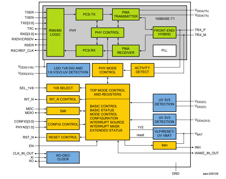
Block Diagram
TJA1101’s block diagram is shown below. The 100BASE-T1 portion includes functional blocks specified in the 100BASE-T-1 standard, which constitute the physical coding sublayer (PCS) and physical medium attachment (PMA) layer of the signal transmission and reception paths. MII/RMII interfaces (including serial management interfaces (SMI)) comply with IEEE802.3 clause 22.
Additional blocks are defined for mode control, register configuration, interrupt control, system configuration, reset control, local wake-up, remote wake-up, under-voltage detection, and configuration control.
Many power-related functional blocks are defined: an internal 1.8V regulator for the digital core, ultra-low power (VLP) supply for sleep mode, reset circuits, power monitoring, and inhibit control.
The clock signal required for PHY operation is generated in the PLL block, derived from an external crystal or oscillator input signal.
Pin bundling allows for many default PHY settings (e.g., master or slave configuration) to be hardware-configured upon power-up.
4.5, Power Management Chips
4.5.1, TPS6594
The TPS6594-Q1 has 5 buck converters and 4 LDOs and is suitable for automotive safety-related applications.
Features
|
Features |
Function |
|
Meets automotive application requirements,with features compliant with AEC-Q100 standard |
– Input power supply voltage range of the device is 3V to 5.5V – Device temperature grade1:–40°C to +125°C Environmental operating Temperature range – Device HBM classification level 2 – Device CDM classification level C4A |
|
Meets functional safety standards
|
– Developed for functional safety applications – Helps make ISO 26262 system design comply with ASIL-D documentation – Helps make IEC 61508 system design comply with SIL-3 documentation – System functions comply with ASIL-D – Hardware integrity complies with ASIL-D – Input power voltage monitoring and over-voltage protection – Under-voltage/over-voltage monitoring and over-current monitoring on all output power rails – Watchdog with optional trigger/Q&A mode – Two error signal monitoring with optional level/PWM mode (ESM) – Temperature monitoring with high-temperature warning and thermal shutdown functionality – Bit integrity (CRC) error detection for internal configuration registers and non-volatile memory |
|
Low Power Consumption
|
– 2μA typical shutdown current – Typical value of 7μA only in backup power mode – Typical value of 20μA in low power standby mode
|
|
Five switch mode power buck regulators:
|
– Output voltage range: 0.3V to 3.34V(Voltage step of 5mV、10mV or 20mV) – Output current:One is 4A, the other three are 3.5A, and one is 2A – Flexible multi-phase feature of four buck regulators:Single rail output current up to 14A – Short-circuit and over-current protection – Internal soft start limits inrush current – Switching frequency of 2.2MHz/4.4MHz – Can be synchronized with external clock input
|
|
Three low dropout (LDO) linear regulators with configurable bypass mode
|
– Output voltage range in linear regulator mode: 0.6V to 3.3V (Voltage step of 50mV) – Output voltage range in bypass mode:1.7V to 3.3V – 500 mA output current,with short-circuit and over-current protection |
|
One low-noise low dropout (LDO) linear regulator
|
– Output voltage range: 1.2V to 3.3V(Voltage step of 25mV) – 300mA output current,with short-circuit and over-current protection |
|
Configurable power sequencing control in non-volatile memory (NVM):
|
– Configurable power-up and power-down sequences between power states – Digital output signals can be included in the power sequence – Digital input signals can be used to trigger power sequence transitions – Configurable safety-related error handling |
|
• 32kHz crystal oscillator with buffered 32kHz clock output • Real-time clock (RTC) with alarm and periodic wake-up mechanism • One SPI or two I2C control interfaces,and the second I2C interface is dedicated to Q&A watchdog communication |
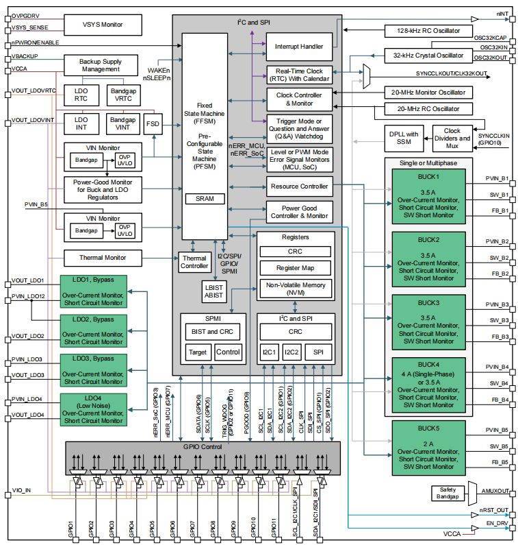
Functional Block Diagram
4.5.2, MAX20087
Introduction to MAX20087
Dual/four-channel camera power protectors; the industry’s only ASIL-rated camera protectors, providing diagnostics via I2C. Maxim has a total of 4 camera power diagnostic chips: MAX20086, MAX20087, MAX20088, MAX20089.
The MAX20086–MAX20089 dual/four camera power detectors ICs provide up to 600mA load current for each of the four output channels. Each output is individually protected against battery short circuits, ground short circuits, and over-current conditions. The IC operates with a power supply of 3V to 5.5V and a camera power supply of 3V to 15V. At 300mA, the voltage drop from input to output is only 110mV (typical).
The IC provides enable inputs and an I2C interface to read the diagnostic status of the device. The onboard ADC can read the current through each switch. Versions compliant with ASIL B and ASIL D support reading an additional seven diagnostic measurements through the ADC, ensuring high fault coverage.
The MAX20086–MAX20089 include over-temperature shutdown and over-current limit on each output channel. The design environment temperature for all devices is -40°C to +125°C.
Features
|
Features |
Function |
|
Small solution size
|
Up to 4 600mA protection switches 3V to 15V input power supply voltage 3V to 5.5V device operating power 26V battery short-circuit isolation Adjustable limit current value(100mA to 600mA) For higher currents, parallel multi-channel OptionalI2C address Small size(4mm × 4mm), 20-pin SWTQFN and WETQFN packages |
|
High precision
|
±8% current limit accuracy 0.5ms soft start time 0.25ms soft shutdown time 0.3µA shutdown current 110mV voltage drop @ 300mA |
|
Designed for safety applications |
Compatible with ASIL B/D Short circuit diagnostics VBAT/GND Output over-voltage/under-voltage diagnostics Input over-voltage/under-voltage diagnostics Read each channel’s 8-bit current, output voltage, and power readings via I2C Automatically retries upon failure |
|
AEC-Q100 certified, -40°C to +125°C operating temperature range |
4.5.2, MAX20087
|
Chip |
Price |
|
DRA829 |
700 |
|
Samsung eMMC5.1 KLM8G1GEUF |
18 |
|
Samsung LPDDR4 K4FBE3D4HM |
100 |
|
Maxim MAX96718F |
100 |
|
Maxim MAX96722 |
110 |
|
NXP 100M PHY transceiver JA1101A |
18*2 |
|
Texas Instruments TPS6594 |
80 |
|
Maxim MAX20087A |
20*2 |
|
NXP TJA1043 |
15*4 |
|
Texas Instruments LM5143 |
50 |
–end–
Sharing is not easy, please give a【👍】and【look】