| 1. SiO₂ nanoparticle doping rate (5-20wt%) | |
| 2. Nanocellulose diameter (10-15nm) | |
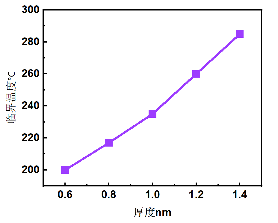
| 3. Metal oxide layer thickness (0.5-2nm) | |
| 4. Organic-inorganic hybrid interface density (10³/cm²) | |
| Micro composition (10 items) | 5. Ultra-thin silicon layer lattice defect density (<10⁵/cm²) |
| 6. Flexible polymer chain orientation (>80%) | |
| 7. Nanowire conductive network porosity (5-30%) | |
| 8. Stress buffer layer Young’s modulus (0.1-5GPa) | |
| 9. Surface roughness (Ra<0.5nm) | |
| 10. Coefficient of thermal expansion (CTE 0.1-5ppm/K) | |
| Macro composition (10 items) | 1. Multi-layer flexible packaging structure (PI/BCB/PET) |
| 2. Ultra-thin silicon-based chip thinning layer (<1.4nm) | |
| 3. Nano-imprinted patterned conductive layer | |
| 4. Biodegradable paper substrate (transmittance >85%) | |
| 5. Strain-isolated serpentine interconnect structure | |
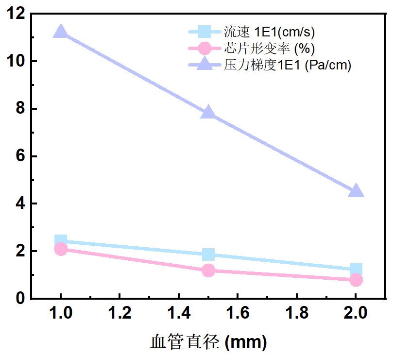
| 6. Stretchable microfluidic channel network | |
| 7. Flexible antenna integrated module (<1GHz bandwidth) | |
| 8. Self-healing polymer coating (repair rate >90%) | |
| 9. Thermal management phase change material layer (thermal conductivity >3W/mK) | |
| 10. Multi-modal sensor array (density >100/cm²) | |
| Function (10 items) | 1. Reduce interface thermal stress (ΔT<50℃) |
| 2. Enhance ductility (>200%) | |
| 3. Suppress crack propagation (critical strain >5%) | |
| 4. Improve electrical signal transmission stability (impedance fluctuation <5%) | |
| 5. Optimize thermal expansion matching (CTE difference <2ppm/K) | |
| 6. Increase transmittance (visible light range >90%) | |
| 7. Achieve biocompatibility (cell survival rate >95%) | |
| 8. Support high-frequency signal transmission (loss <0.1dB/mm) | |
| 9. Dynamic stress self-adaptive adjustment (response time <1ms) | |
| 10. Extend cycle life (>10⁵ bends) | |
| Location (10 items) | 1. Chip-substrate interface layer |
| 2. Stress buffer transition zone | |
| 3. Conductive interconnect topology network | |
| 4. Packaging protective outer layer | |
| 5. Thermal management functional interlayer | |
| 6. Sensor integration surface | |
| 7. Wireless communication module embedded layer | |
| 8. Biological tissue contact surface | |
| 9. Environmental response smart coating | |
| 10. Energy harvesting unit integration area | |
| Value (10 items) | 1. Reduce manufacturing costs (30% lower than silicon-based processes) |
| 2. Increase device density (integration +50%) | |
| 3. Promote commercialization of wearable medical devices | |
| 4. Achieve breakthroughs in electronic skin human-computer interaction | |
| 5. Accelerate deployment of IoT edge computing | |
| 6. Break through traditional chip mechanical performance limits | |
| 7. Support heterogeneous integration (compatible with 5 types of materials) | |
| 8. Reduce electronic waste (biodegradation rate >80%) | |
| 9. Improve energy efficiency (power consumption reduced by 40%) | |
| 10. Open up flexible electronics applications in space | |
| Significance (10 items) | 1. Break through the physical limits of Moore’s Law |
| 2. Promote iteration of flexible display technology (folding radius <1mm) | |
| 3. Achieve long-term implantation stability of brain-machine interfaces | |
| 4. Solve the mechanical mismatch problem in human-computer interaction | |
| 5. Promote sustainable development of green electronics | |
| 6. Build ubiquitous sensing IoT infrastructure | |
| 7. Support miniaturization of AI terminal devices | |
| 8. Innovate real-time monitoring patterns in medical diagnostics | |
| 9. Promote lightweight design in aerospace | |
| 10. Open a new era of wearable devices in the metaverse |
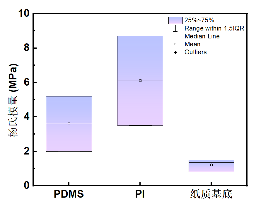
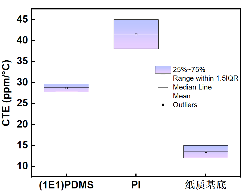
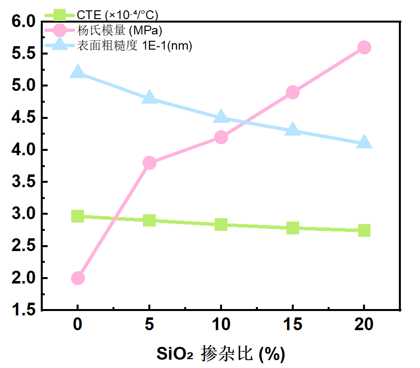
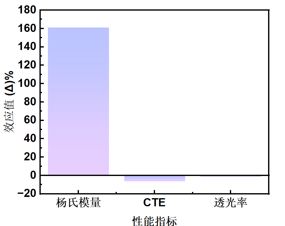
Performance ParametersComparison of substrate material performance, parameter changes at SiO₂ doping amount of 16.18%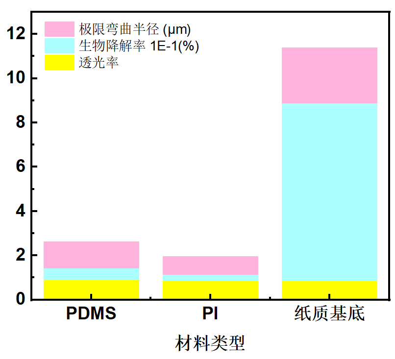
Impact of SiO₂ Doping Gradient
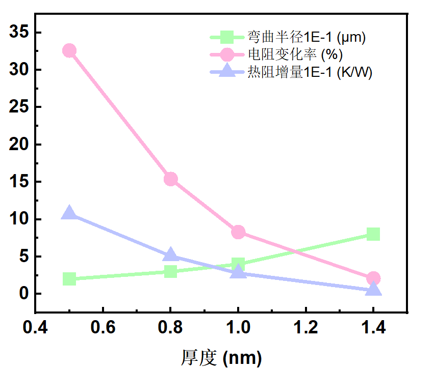
Chip Thickness and Performance Degradation
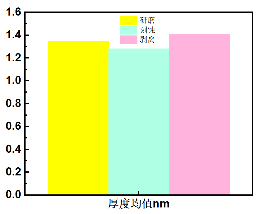
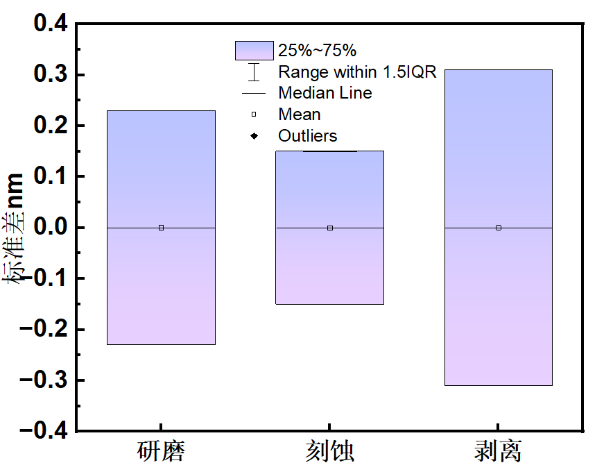
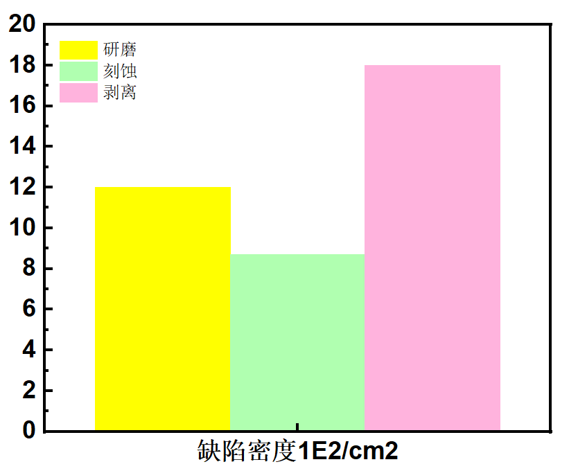
Thinning Process Discreteness
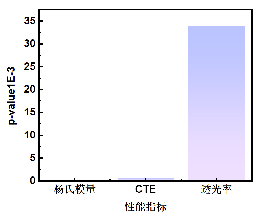
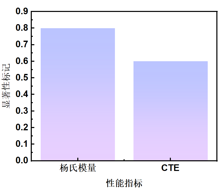
Significance Screening
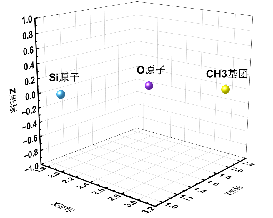
PDMS-Si O₂ Interface Atomic Coordinates
LSTM Thermal Stability
Fluid Dynamics
 END
END Follow Us