1. General Practices
When designing PCBs, in order to make the design of high-frequency, high-speed, and analog circuit boards more reasonable and improve anti-interference performance, the following aspects should be considered:
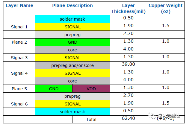
(1) Reasonable selection of layer count; in PCB design for high-frequency and high-speed circuit board routing, using the inner layer planes as power and ground layers can play a shielding role, effectively reducing parasitic inductance; it can also reduce cross-interference between signals.
(2) Routing method; routes should turn at 45° angles or use curved corners to reduce reflections and coupling between high-frequency and high-speed signals.

(3) Routing length; unless there are specific requirements, shorter routing lengths are better (for loss requirements, it should be based on actual conditions); for adjacent routing, the shorter the parallel distance between lines, the better.
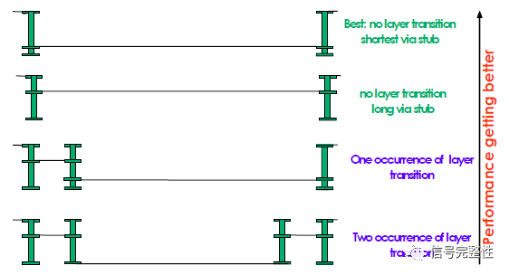
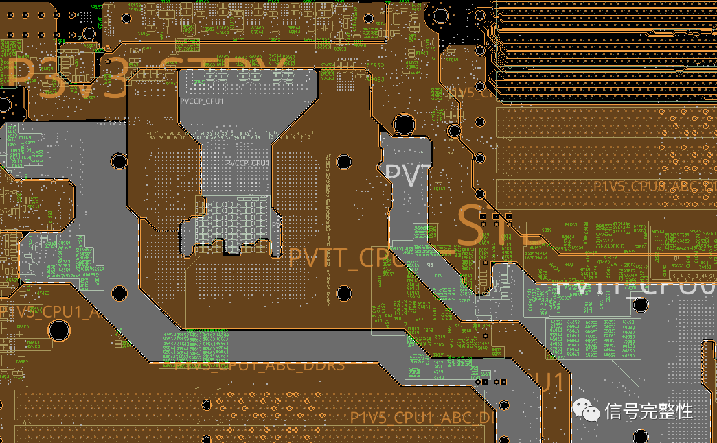
(4) Via design and quantity; when designing vias, try to ensure that the impedance of the vias is consistent or as close as possible to the impedance of the transmission lines; at the same time, fewer vias are better, as vias can easily cause impedance discontinuities.
(5) Routing direction between adjacent layers; the routing direction between layers should be perpendicular, with the upper layer being horizontal and the adjacent layer being vertical, to reduce interference between signals.
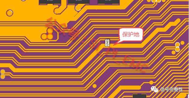
(6) Grounding; many times, engineers believe that grounding important signal lines can significantly improve the anti-interference ability of those signals, but it is essential to avoid introducing new problems, such as whether it leads to reduced space or changes in impedance. Of course, grounding can also be applied to interference sources to prevent them from interfering with other signals. Whether to protect the ground line in high-speed PCB design is a question.
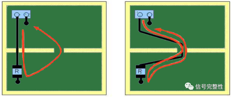
(7) Signal lines; signal routing should not form loops to reduce noise introduction.
2. Routing Priority Order
Key signal lines take priority: analog small signals, high-speed signals, clock signals, and synchronous signals should be routed first. Density priority principle: start routing from the most complex connection relationships on the board. Begin routing from the most densely connected areas on the board. Points to note: a. Try to provide dedicated routing layers for clock signals, high-frequency signals, sensitive signals, and other key signals, ensuring the smallest loop area. If necessary, manual routing, shielding, and increasing safety distances should be employed to ensure signal quality. b. The EMC environment between power and ground layers is poor, so avoid placing interference-sensitive signals. c. Networks with impedance control requirements should be routed according to line length and width requirements.
3. Clock Routing
Clock lines are one of the factors that have the most significant impact on EMC. There should be few vias on clock lines, and they should avoid running parallel to other signal lines and be kept away from noise sources or heat sources to prevent interference with signal lines. They should also avoid the power section on the board to prevent interference between power and clock.
If there is a dedicated clock generation chip on the board, no routing should be done beneath it; copper should be laid under it, and if necessary, grounding can be done specifically. For many chips, there are reference crystal oscillators, and no routing should be done under these crystals; copper should be laid for isolation.
(1) Clock driver layout should be at the center of the PCB rather than at the edge of the board, and the layout should be as close as possible, with smooth and short routing, avoiding right angles and T-shaped connections.
(2) Avoid interference between clocks and between signals, and avoid parallel routing of several signals. If necessary, use GND shielding layers for isolation, maintaining a significant distance between different clocks or signals.
(3) Clock signals should avoid crossing plane splits.
(4) If it is a differential clock line, ensure that they are of equal length.
(5) Clock crystal: the clock line should first go through the load capacitors before reaching the crystal, with vias around it, and GND shielding.
(6) Common clock: the parallel matching resistance of the clock line should be close to the load chip, and the series resistance should be close to the clock chip or CPU.
4. Right Angle Routing
Right-angle routing is generally a situation that should be avoided in PCB routing and has almost become one of the standards for measuring routing quality. So how much impact does right-angle routing have on signal transmission? In principle, right-angle routing can cause changes in the width of the transmission line, leading to impedance discontinuity.
In fact, it is not only right-angle routing but also abrupt angles and sharp angles that can cause impedance changes.
The impact of right-angle routing on signals mainly manifests in three aspects: first, corners can be equivalent to capacitive loads on the transmission line, slowing down the rise time; second, impedance discontinuity can cause signal reflections; third, sharp corners can generate EMI.
5. Differential Routing
Differential signals are increasingly used in high-speed circuit design, with the vast majority of signals in circuits adopting differential line structures.

The use of differential lines is intended for anti-interference, and its advantages can be explained from two perspectives.
First, for signals with the same amplitude level, the peak-to-peak value of differential lines is twice that of single-ended lines.
Second, in the same circuit environment, single-ended routing references the ground plane, which shows significant differences in interference from external sources compared to the same disturbance on the ground plane, leading to interference on routing and return paths that cannot cancel each other out (the voltage reference for single-ended routing is the ground plane); whereas differential lines, being parallel and of equal length, have a high coupling degree in the same circuit environment, and when subjected to the same interference source, the interference levels on both lines are similar, with the differential line voltage reference point being the corresponding other line instead of the ground plane, providing better common-mode interference suppression.
To achieve higher anti-interference capability and lower bit error rates, differential lines require an additional line as a return path for the signal. Therefore, only in designs that pursue higher transmission rates or stronger anti-interference capabilities will the number of transmission lines be increased to ensure transmission speed and stronger anti-interference capabilities.
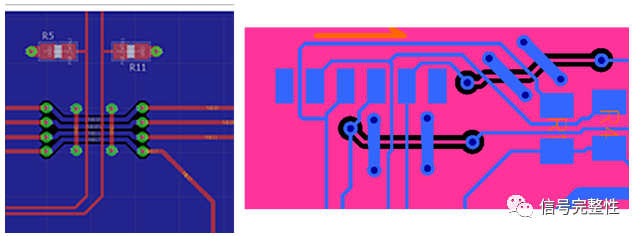
For PCB engineers, when designing differential transmission lines, it is essential to maintain equal lengths and consistent impedance (equal spacing) within the differential pair.
Equal length is to ensure that the two differential signals maintain opposite polarities at all times, reducing common-mode components; equal spacing is primarily to ensure that the differential impedances are consistent, minimizing reflections. As for the commonly discussed tight coupling versus loose coupling, it depends on the situation. Is tight coupling really better than loose coupling?
6. Serpentines
Serpentines are a frequently used routing method in layout design. Their primary purpose is to adjust the delay of transmission lines, especially to meet the equal length requirements for internal or interconnections, or to meet specific system timing requirements.
7. Power and Ground Line Management
Even if the routing throughout the PCB is done well, interference caused by inadequate consideration of power and ground lines can degrade product performance and sometimes even affect the success rate of the product. Therefore, careful attention should be paid to the routing of power and ground lines to minimize noise interference, ensuring product quality.
The PCB routing rules for ground and power lines are as follows:
1. Add decoupling capacitors between power and ground.
2. Widen the power and ground line widths as much as possible, preferably making the ground line wider than the power line.
3. In high-speed digital circuits, use wide ground lines to form a loop, and it is best to have a complete ground plane for reference. This cannot be done for analog circuits.
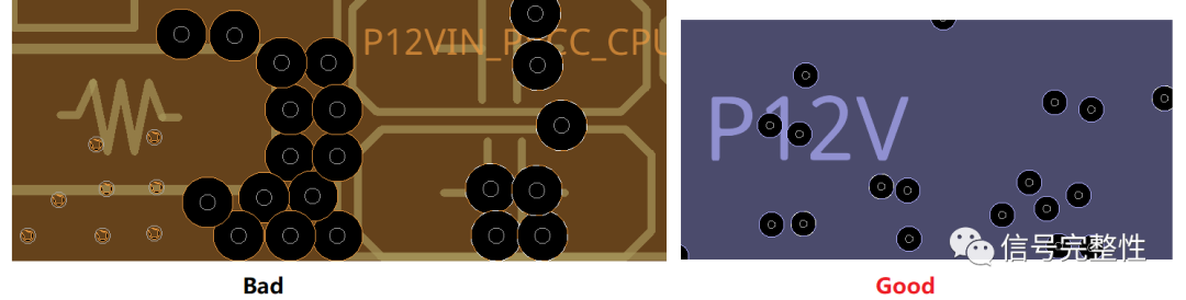
4. Use large copper areas for ground lines, connecting unused areas on the printed board to ground, or create a multi-layer board, with each layer dedicated to power and ground.
5. In areas with dense vias, avoid connecting vias in the power and ground layers’ hollowed-out regions, which can disrupt the integrity of the plane layer and increase the loop area of signal lines in the ground layer.
Ground Loop Rules:
The ground loop should be as small as possible, meaning that the loop area formed by the signal line and its return path should be minimized. The smaller the loop area, the less radiation it emits, and the less noise it receives from external interference.
Decoupling Capacitor Rules:
A. Add necessary decoupling capacitors on the PCB to filter out interference signals on the power supply, stabilizing the power signal. The layout of decoupling capacitors and the routing method of the power supply will directly affect the stability of the entire system, sometimes even determining the success of the design.
B. In PCB design, current should generally pass through filtering capacitors before being used by devices.
C. In high-speed circuit design, correctly using decoupling capacitors is critical for the stability of the entire board.
8. Common Ground Handling for Digital and Analog Circuits
Many PCBs today are no longer single-function circuits (digital or analog) but are composed of mixed digital and analog circuits. Therefore, when routing, it is essential to consider the interference issues between them, especially noise interference on the ground.
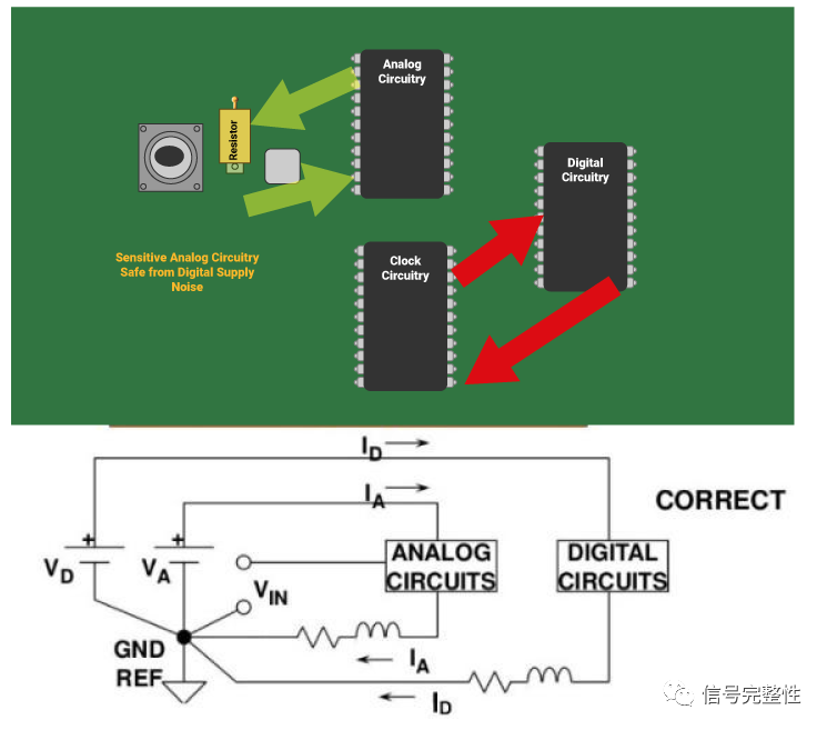
Digital circuits operate at high frequencies, while analog circuits are highly sensitive. For signal lines, high-frequency signal lines should be kept as far away as possible from sensitive analog circuit components. For ground lines, the entire PCB should have only one node to the outside, so the problem of common ground for digital and analog circuits must be handled internally on the PCB. Internally, the digital and analog grounds are actually separated and not interconnected; they only connect at the interface with the outside (such as connectors). The digital ground and analog ground should only have one connection point. There are also cases where there is no common ground on the PCB, which depends on the system design.
9. Signal Lines Routed on Power or Ground Planes
In multi-layer PCB routing, if there are not many remaining lines to route on the signal layer, adding more layers will cause waste and increase the workload for production, which also increases costs. To solve this contradiction, consider routing on the power and ground plane layers. The power layer should be prioritized, followed by the ground layer, as it is best to maintain the integrity of the ground plane.
10. Design Rule Check (DRC)
After completing the routing design, it is necessary to carefully check whether the routing design conforms to the rules set by the designer and also to confirm whether the established rules meet the production process requirements for the printed board. The general checks include the following aspects:
(1) The distances between lines, between lines and component pads, between lines and vias, between component pads and vias, and between vias should be reasonable and meet production requirements. (2) Are the widths of power and ground lines appropriate? Are the power and ground planes tightly coupled? (3) Have optimal measures been taken for critical signal lines, such as length, protective lines, and the distances between transmit (TX) and receive (RX) lines (some require layered routing)? (4) Do the analog and digital circuit sections have their own independent ground or how are they connected? (5) Are there process lines added on the PCB? Does the solder mask conform to production process requirements, is the solder mask size appropriate, and are character marks pressed onto component pads to avoid affecting assembly quality? (6) In multi-layer boards, should the outer frame edges of the power and ground layers be reduced, as exposed copper foil could easily cause short circuits?
11. Check 3W and 3H Principles
The 3W principle refers to the center spacing between signal lines being three times the line width.
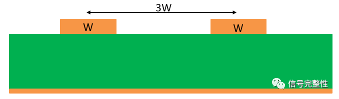
The 3H principle refers to the center spacing between signal lines being three times the distance from the signal line to the reference layer.
Whether it is the 3W or 3H principle, both are aimed at reducing crosstalk between signal lines, especially between high-speed or high-frequency signal lines. As long as the 3H or 3W principles are satisfied, crosstalk will be minimal. However, for miniaturized product designs, it is already challenging to meet the 3W or 3H principles. Moreover, the primary sources of crosstalk are no longer just the influence between transmission lines.
For PCB design, there are various opinions, and every engineer has their understanding.
Finally, I recommend Teacher Jiang’s work—ADS Signal Integrity Simulation and Practice
Note: The article is reproduced from the Signal Integrity WeChat public account, and the copyright belongs to the original author. RF Academy only authorizes forwarding on the WeChat public platform; any reproduction or crawling on other websites must be contacted with the original author.
【RF Introduction】【Chip Filter】