ver0.2
Introduction
In previous articles, we briefly introduced the Power Control Framework (PCF) and understood the main functions of its core components, which revolve around two key concepts: “power domains” and “power modes”. Building on this foundation, this article will further explore the concept of granular “domains” controlled by the SCP for various agents. Modern SoC systems are becoming increasingly complex, integrating a large number of IPs. Taking the CPU as a functional unit, the mainstream heterogeneous architectures in the market typically have at least 8 PE-Cores. When busy, the CPU’s main frequency must be increased for full performance, while during idle times, it is necessary to lower the CPU frequency or even turn off some PE-Cores to conserve power while maintaining sufficient computational capacity. This process may seem straightforward, but it is quite complex, especially in heterogeneous architectures where different PE-Cores belong to different clusters, each with varying frequencies and computational power. To achieve control based on scenarios, precise management is required from the SCP, which involves subdividing all functional units on the SoC into specific “domains”. These are further categorized into voltage domains and power domains based on different modes and control methods. Before reading this article, we hope you will review our previous articles to grasp some basics and get a feel for the topic:
(1) [V-02] Basics of Virtualization – CPU Architecture (based on AArch64)
(2) [A-03] ARMv8/ARMv9 – Multi-level Cache Architecture
(3) [A-21] ARMv8/v9 – Overview of SMMU System Architecture and Functions
(4) [A-25] ARMv8/v9 – System Architecture of GIC (Hardware Foundation of Interrupts)
(5) [A-38] ARMv8/v9 – Generic Timer System Architecture
(6) [A-41] ARMv9/v8 – Power Management System Architecture
(7) [A-42] ARMv9/v8 – Overview of Power Management Operation (SCP Service Overview)
(8) [A-43] ARMv9/v8 – Introduction to Power Control Framework (PCF)
Main Text
1.1 Background
Let’s take a moment to study our own home circuit system, as shown in Figure 1-1.
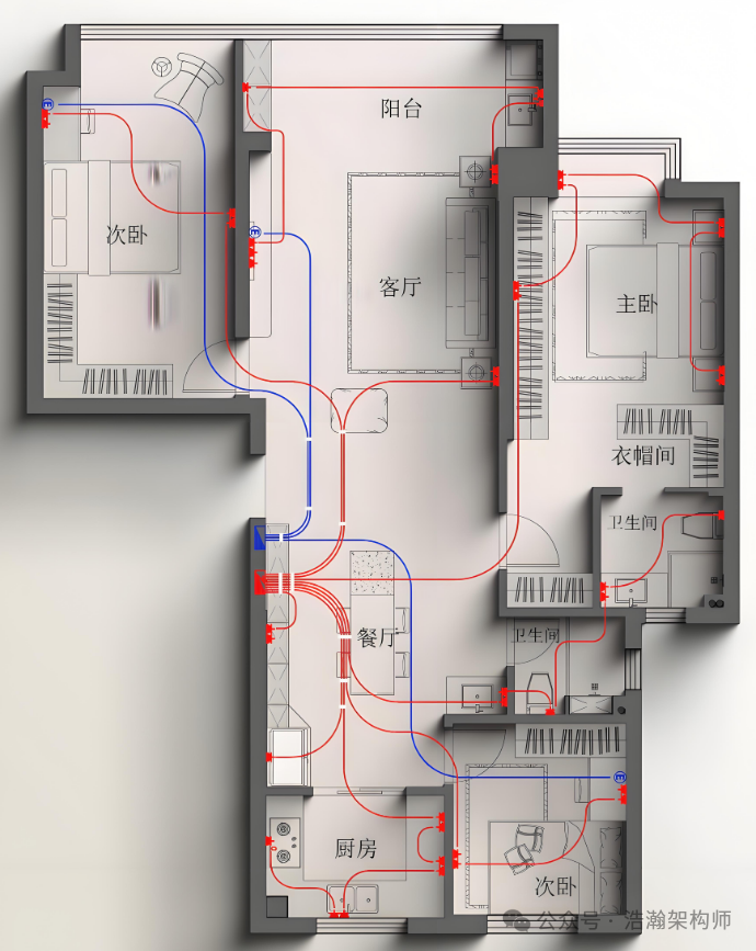
Figure 1-1 Home Circuit System
The above is a typical home circuit system. Let’s analyze its characteristics:
(1) There is a distribution box at the entrance, which extends the circuit to various rooms through wiring, with each room’s wiring connecting various household appliances through sockets (interfaces).
(2) Each room is an independent high-voltage area, isolated from each other through the distribution box’s branch circuit and leakage protection devices, ensuring that the working state of the kitchen circuit does not affect the bedroom or living room circuits.
(3) Standardized interfaces allow compliant appliances to connect seamlessly to the home circuit, and each appliance can internally adjust the voltage to appropriate levels or convert AC to DC.
(4) With the rise of smart homes, the control of home circuits has become more intelligent, no longer limited to ON/OFF states, albeit at a higher cost.
We are not professional high-voltage engineers, so we can only summarize briefly, but an important power management concept emerges: centralization and zoning (areas), which can be further subdivided into smaller areas for individual management if necessary.
Now, let’s shift our perspective to the SoC. If the SoC is a house, it is a very large and complex one, so complex that ARM has developed the PCF framework to facilitate integration work. Let’s first look at the complexity of this house by examining a small room, as shown in Figure 1-2:
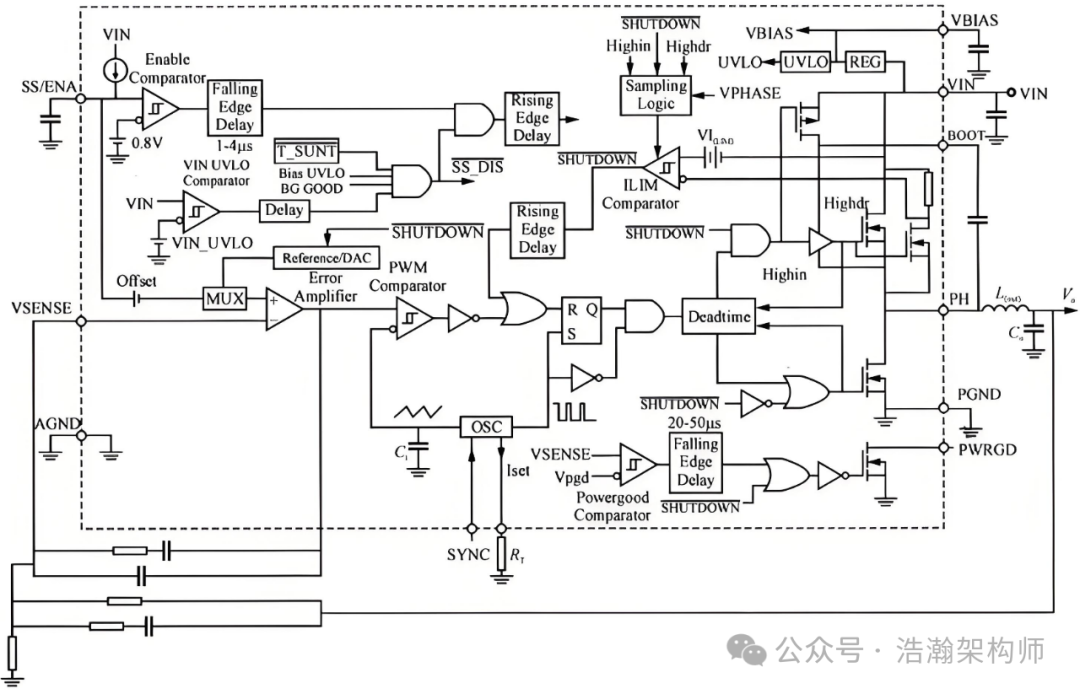
Figure 1-2 High-Level IP Logic Circuit Demo
The above is just a high-level logic link example of a simple IP-Core. We are not electrical or hardware engineers, so we do not need to understand it fully; we just need to know that it is complex enough. Now let’s look at the “grandeur” of this big house, as shown in Figure 1-3:
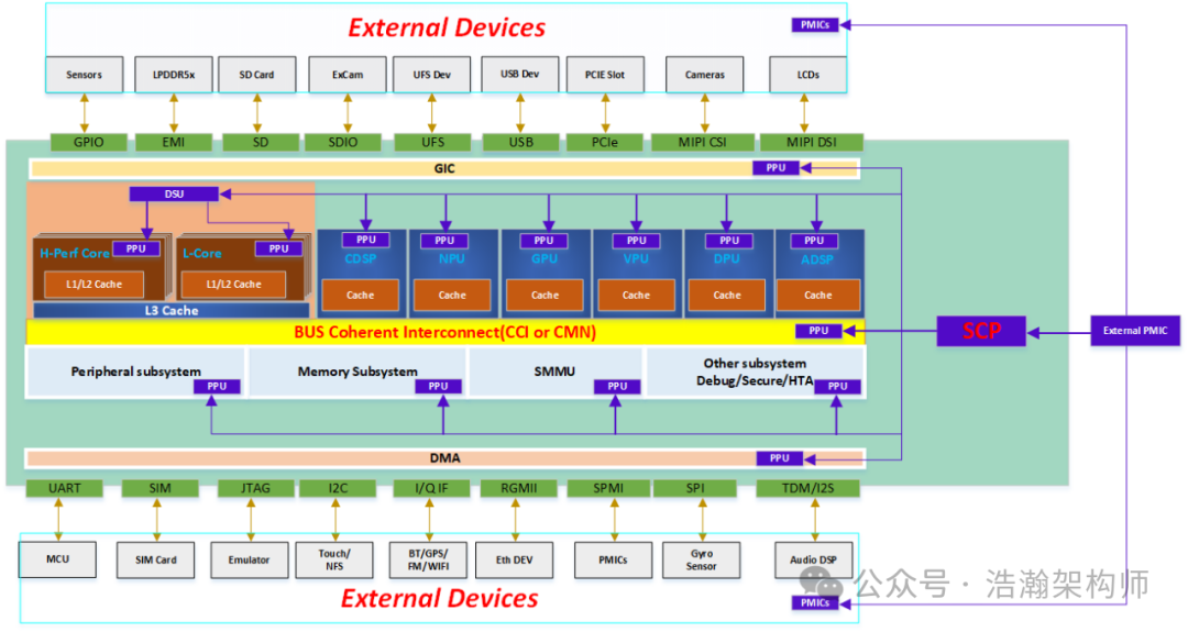
Figure 1-3 High-Level SOC Power Management Framework
This is a high-level system architecture diagram of power management for the SoC. It may not be particularly rigorous, but it sufficiently illustrates the issue. The SCP is the center of power management, while the various IPs on the internal bus of the SoC represent individual rooms, with the SCP managing the power states of each room through the PPU agent.
The theme of our discussion today is about these “rooms” on the SoC. Even with a 90 square meter house, some developers design it as three bedrooms, one living room, one kitchen, and one bathroom, while others may create two bedrooms, one living room, one kitchen, and one bathroom. Today, let’s see how the SoC, this big house under the ARM architecture, is divided into rooms. Regardless of how it is divided, the CPU, as the brain of the SoC, is undoubtedly the most important room, which we will briefly introduce below.
1.2 Voltage Domain
1.2.1 Concept of Voltage Domain
Now that we have the big house of the SoC and have customized the layout, how should this layout be defined? Let’s first look at the description in the manual:
A voltage domain is defined here as a collection of design elements supplied by a single voltage source. The voltage supply to the domain might be scaled or removed for power or performance reasons.
In practice, a SoC can have many voltage supplies across logic domains, I/O, and analog functions. While a single logic voltage supply could be used for all the SoC, this is now rarely the case except in low complexity solutions.
A primary motivation for additional voltage domains is to support DVFS for functional areas of the SoC. DVFS is a fundamental technique for both energy and performance optimization. While initially used for AP cores, it is increasingly being applied to other components of the SoC.
A second motivation can be to enable external supply switch-off, or reduction to non-functional state retention levels, to some logic areas while maintaining an operational level supply to others. This approach can be used both as complementary to and as a substitute for on-chip power gating.
From a cost perspective, the addition of voltage supplies can be significant since additional voltage regulators are required, and extra effort and complexity are required in the SoC physical implementation. A consequence of these factors is that the function size, or area, required to justify a voltage domain is significant. Therefore, the value of the addition of each voltage domain must be carefully assessed against the performance and power requirements for the design.
Let’s interpret the above description from the manual:
(1) The SOC system can be divided into different areas based on independent voltage sources. All elements (all circuits) within a voltage domain operate at the same voltage, and the voltage source can be independently adjusted (scaled or removed) for power and performance reasons.
(2) In practice, a SoC will be divided into different voltage domains. A system with only one voltage domain is now very rare, especially in mobile devices such as smartphones, tablets, or devices that need to support low-power operating modes, such as the increasingly popular smart cockpit and intelligent driving systems in electric vehicles.
(3) For the SoC, dividing voltage domains provides an important means to optimize the overall system’s energy efficiency and performance, which is DVFS (Dynamic Voltage and Frequency Scaling). DVFS technology has been widely applied to CPUs and is gradually transitioning to other IPs, such as GPUs, NPUs, VPUs, etc.
(4) Another benefit of dividing voltage domains is that it allows for the complete shutdown of power to certain areas of the SoC while maintaining normal power supply to other voltage domains, thereby reducing power consumption. (Those who have developed STR functionality should be familiar with this; the core metric of STR is the dark current during system sleep. How low have you optimized it to, haha.)
(5) Since there are so many benefits to dividing into different voltage domains, wouldn’t it be better to subdivide all functional units of the SoC into independent voltage domains? Not necessarily; there are costs involved. The more voltage domains there are, the larger the board size and the more complex the wiring, making integration more challenging. The number of voltage domains should be reasonable, primarily based on demand and the design capabilities of the chip manufacturers.
Let’s look at an example to help further understand the concept of voltage domains, as shown in Figure 1-4:
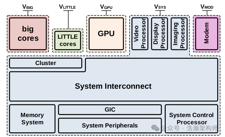
Figure 1-4 Voltage Domains: Mobile SoC example
1.2.2 Division of Voltage Domains
Figure 1-4 shows the division of voltage domains in a Mobile SoC, which is a schematic diagram. There is no need to be overly precise; in reality, just the CPU block would be divided more finely, haha. Each domain is represented by a separate color, and the elements within each domain operate at the same voltage, subject to the same voltage adjustments. As mentioned earlier, the division of voltage domains must consider various factors, especially cost. However, the manual also provides some guidance on the minimum voltage domain considerations for a SoC:
System Logic (V-SYS)
A SoC will have some shared system logic functions typically composed of interconnect, memory system, peripherals, and other shared infrastructure.
It is convenient to consider the voltage supply for these functions as the default supply for the SoC. The exact functions contained within this voltage domain depend on the choices taken to support additional voltage domains for each function. This supply is referred to here as V-SYS.
Always-On Logic
Always-on logic is required so the SoC can be woken from sleep states.
The supply to the always-on logic of the SoC is typically the main system logic supply (V-SYS).
However, a second common strategy is the provision of a dedicated supply for this logic. This is one case where the size of a voltage domain might be small.
Processor Clusters
Cortex-A profile processor clusters in most markets, and invariably in mobile SoCs, will have dedicated voltage domains to enable DVFS.
In an Arm DynamIQ TM based big.LITTLE system, a single cluster supports both core types. The cluster in these systems is recommended to use a voltage supply independent of the big and LITTLE core supplies. This might be the main logic supply (V-SYS) or as part of a scaled memory system voltage supply.
In applications where DVFS is not required, or the cost is too high, then the processor cluster is in the V-SYS domain.
In some applications, such as modems, Cortex-R profile processor clusters might also be given dedicated voltage domains.
Graphics Processor
Graphics processing performance in mobile applications has grown significantly and is anticipated to continue. GPU workloads represent throughput processing, with very high inherent parallelism, and are well suited to using DVFS to adapt the performance and energy profile of a given hardware configuration to a frame level deadline.
These properties also enable adaptation to different requirements. Cost-centric designs can implement fewer cores at higher frequency and voltage, while energy-performance-centric designs can implement more cores at lower frequency and voltage.
Therefore, a dedicated voltage domain to enable GPU DVFS is often implemented to enable these benefits.
In applications where DVFS is not required, or the cost is considered to outweigh the benefit, then the GPU cluster is in the V-SYS domain.
Other Functions
Further voltage domain partitions are less common as the cost to benefit ratio and implementation feasibility degrades.
One example might be an integrated modem, which is effectively a system within a system, as this is a function of significant size. In this case, motivation can arise from the potential for scaling, according to mode or required performance, and for independent powering when other functions have their voltage supply externally shut-off.
A second set of possibilities, for DVFS scaling reasons, could arise from other media processing functions, such as video and display subsystems, or a domain dedicated to a large accelerator such as for imaging.
As in the previous cases, all functions that do not have dedicated domains are in the V-SYS domain.
Let’s summarize briefly:
(1) The number of voltage domains in a SoC should consider cost and benefits, but there must be a baseline: there must always be a fallback voltage domain V-SYS, which controls all logic units that cannot be independently formed into domains.
(2) The system must have an Always-ON module responsible for managing the power subsystem of the entire SoC even in low-power modes. This is similar to our previous summary of the home circuit system, where there must be a central point in power management. In the ARM architecture, this central point is the SCP. Other IPs and functional units on the system can sleep or even be powered off, but the Always-ON functional unit must always keep one eye open to monitor the dynamics of the entire SoC system, quickly responding to relevant events to restore the functionality of other voltage domain units, such as lighting up the screen.
(3) The CPU is always a major consumer of energy within the SoC, as it is crucial, much like the human brain, consuming a lot of energy when it operates. If it consumes too much, we need to optimize its energy consumption during operation, and the method is DVFS technology. The goal is to extend the operational time of a SoC with the same energy.
(4) Even without the current hot concept of large models, the GPU deserves to be separated into its own voltage domain for individual management. Whether in consumer electronics or automotive fields, GPUs are becoming increasingly important, with tedious tasks gradually being offloaded from CPUs to GPUs. GPUs are designed to be larger, with more powerful computing capabilities and richer functional units integrated within a single GPU, but this also leads to greater power consumption. Given this background, GPUs, like CPUs, also require separate voltage domains to facilitate real-time adjustments of their operational states through DVFS.
(5) Other IPs within the SoC should be considered for independent voltage domain division based on circumstances and needs, such as VPUs and DPUs. In other words, if the chip company has strong technology, they will have the motivation to subdivide voltage domains more finely; if they lack that technical reserve, they can simply use ARM’s public version solutions.
1.2.3 Example of Voltage Domain
Let’s look at an example of a voltage domain, as shown in Figure 1-5:
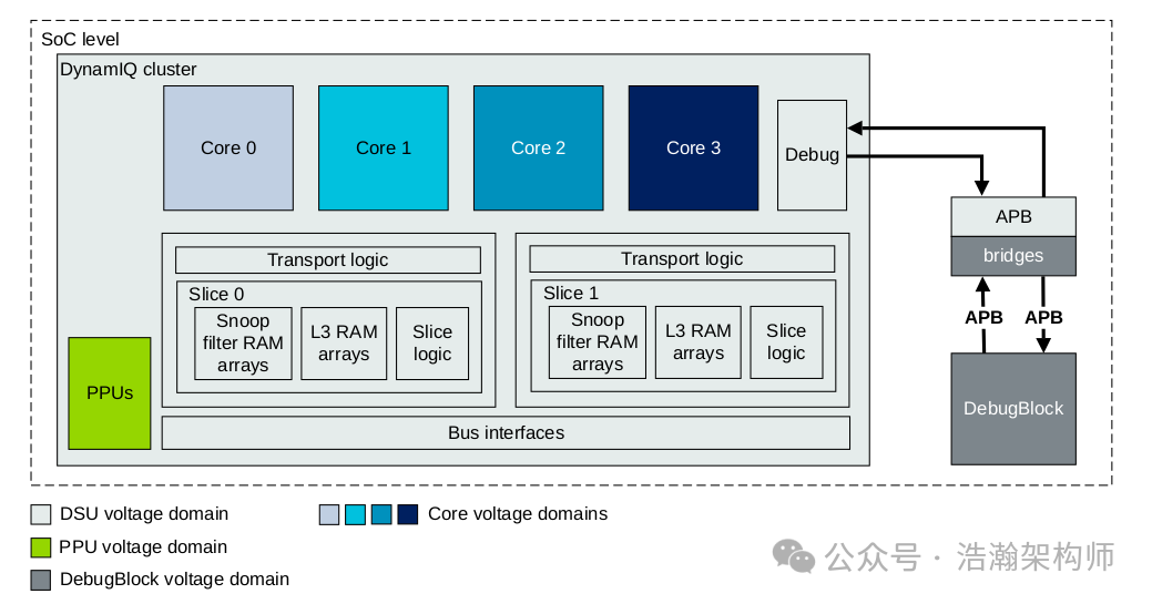
Figure 1-5 DSU-110 Voltage Domains
Applying the characteristics of voltage domains we discussed earlier, let’s summarize the voltage domains of the DSU Cluster:
(1) The DSU has a total of 6 voltage domains: Core0, Core1, Core2, Core3, PPUs, and DSU.
(2) Different voltage domains imply independent power sources, allowing DVFS technology to more finely control each PE-Core within the DSU, balancing power saving and performance needs.
1.3 Power Domain
1.3.1 Concept of Power Domain
Let’s further subdivide the various rooms in our house. The kitchen has a refrigerator, induction cooker, electric oven, rice cooker, etc., all of which require independent ON/OFF switches. The refrigerator’s operating mode is even more complex; besides ON/OFF, it also requires the compressor to operate, meaning that when the compressor is not working, the refrigerator is still powered on, but its overall power consumption is lower. Thus, the power modes of the refrigerator are ON/LOW/OFF.
A power domain is defined here as a collection of design elements, within a voltage domain, that share common power control. A voltage domain can be partitioned into one or more power domains.
Specifically, a power-gated domain is a power domain whose power can be removed by on-chip power switches. A voltage domain can then be partitioned into one or more power-gated domains as well as an always-on (non-gated) power domain.
The motivation for partitioning a voltage domain into several power domains is to facilitate techniques for static leakage power mitigation. These include modes where power is removed, with loss of context, and low leakage retention modes which keep some or all context.
The following subsections describe:
• The power modes that can be supported by a power domain.
• The choice of which power domains to implement in an Arm based SoC.
• Power domain partitioning requirements that must be respected. These include availability and power ordering relationships between vital components in the system.
Let’s interpret ARM’s thinking:
(1) Based on voltage domains, ARM further subdivides its internal functional units, leading to the concept of power domains. Depending on the granularity of the voltage domain and requirements, a voltage domain can be subdivided into one or more power domains, as shown in Figure 1-6.
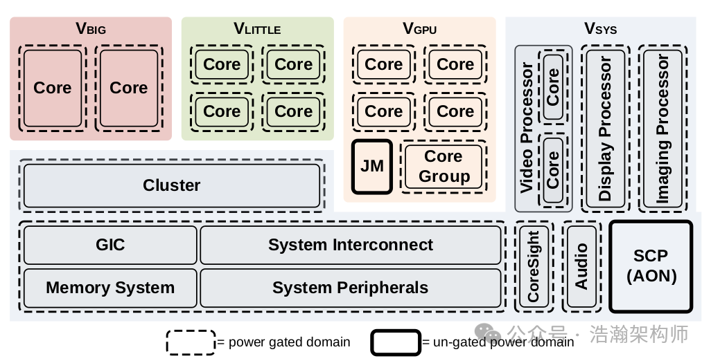
Figure 1-6 SoC Voltage and Power Domain Partitioning Example
(2) Power domains are categorized into always-on (non-gated) power domains, which are always powered on as long as the voltage supply to the domain is normal, keeping all functional units within this domain operational. The other type is the power-gated domain, where the power can be controlled by a switch in the circuit, with one end connected to the voltage source and the other end to the circuit. This switch is special; when it is closed, the circuit is ON, and when it is opened, the circuit is OFF.
(3) Considering some special operational requirements, such as when a user wants the phone to wake up quickly from a black screen with just a light touch on the screen or power button, rather than waiting for a long boot process each time, additional designs must be added to the power-gated circuit to allow for states beyond ON/OFF. This state can retain some necessary state information, enabling the core IP to quickly resume operation after being powered back on. We will tentatively call this state RETENTION. The operational modes and states of power domains are key areas of our study, which we will analyze in detail later:
ON
A power domain always supports an ON mode. This is the normal functional mode for the logic in the power domain. If the power domain supports DVFS, this is applied while the power domain is in this mode. This mode will normally also use clock gating and other techniques to reduce dynamic power consumption.
OFF
A power domain typically supports an OFF mode through the inclusion of on-chip power switches. The power switches are used to remove the power supply when its function is not required.
Retention (RET)
Retention modes offer leakage power reduction without loss of state.
There are several possible RET mode implementations and use models. RET modes can be categorized by the following criteria:
• Entry to and exit from the mode: This can be either hardware autonomous or software visible.
• Physical implementation: Full or partial state retention within the mode.
For a hardware autonomous RET mode, that is transparent to software, all state that is required to resume operations on exit from the mode must be retained by the hardware. Other state can be discarded and so, while from a functional perspective the mode provides apparent full retention, there can be partial state retention from an implementation perspective.
For a software visible RET mode, an explicit software decision is taken to choose the mode, and this means that some context management might be handled by software at entry to and exit from the mode. An example of this is when only specific RAM content will be retained while all other hardware state is discarded. From an implementation perspective, these modes might require only partial retention capability.
(4) Since additional gating circuits are introduced, a dependency relationship arises (note that this refers to a logical perspective). If there are two gates on a circuit, the function of the lower gate depends on the state of the upper gate. If the upper gate is always in the OFF state, then the lower gate cannot function even if it switches to the ON state. Those who have read our articles on multi-level cache architecture and CPU architecture should be familiar with this view; each PE-Core must pass through the cluster circuit (DSU) to connect to the bus and integrate into the SoC system, as shown in Figure 1-7:
Figure 1-7 High-Level DSU Framework
PE-Cores wrapped by the DSU must wait for the DSU to be powered on before they can operate normally. Therefore, one possible implementation is shown in Figure 1-8:
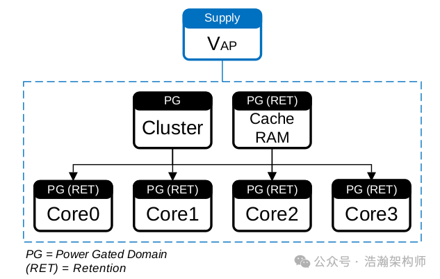
Figure 1-8 Processor Power Domains Example (Logical View)
The relationship between this dependency and power management operational modes is closely related, and we will not elaborate on it here; we will analyze it in detail in future articles.
1.3.2 Division of Power Domains
So how should power domains be divided within a SoC?
Power Domain Choices
The fundamental aim of the power domain strategy is to minimize the powered-on area in each scenario.
From a practical perspective, implementation and control overhead constraints mean that a power-gated domain is typically large with the content representative of significant functions.
When choosing power domains, it is important to consider end use cases to ensure the low-power modes of the chosen domains can be used effectively. Although there can be many detailed use cases, they can normally be reduced to broader classes of usage. From analysis, the opportunity to power-off functions that are not required for significant periods of time can be determined.
Also, the power modes supported by a power domain need to be mapped to one of an explicit set of software power states, or an autonomous mechanism supported by a component. Where the power state control is required to be managed by software, the viability of using an available framework or device driver should also be assessed.
Let’s briefly analyze the principles provided by ARM:
(1) The purpose of establishing power domains is to turn off unnecessary functional units on the SoC in various scenarios. For example, when a user is listening to music with the screen off, there is no need for the GPU, VPU, and other IPs on the SoC to operate at full load; they can be turned off or set to low-power states.
(2) SOC nodes managed by gating are usually high power-consuming nodes, such as CPUs and GPUs, so they need to be controlled finely to achieve a balance of energy efficiency.
(3) The choice of operational modes for power domains must consider the efficiency of recovering to normal operational modes. This also requires a balance. Simply put, OFF is the most power-saving but the slowest to recover to normal operational mode, while RET modes recover the fastest but are more complex to implement, requiring the ability to save and restore context and consuming some additional current.
(4) The operational modes of power domains need to be mapped to the OSPM power states, facilitating software involvement in management, as software understands user intentions best. By involving OSPM in management, the product capabilities of the SoC can be optimized.
So what specific considerations are there for the division of power domains under the ARM architecture?
System Logic
Many of the common system logic functions such as interconnect, memory system, peripherals, and other shared infrastructure will be required during all activity outside of SoC sleep states. A typical SoC gathers these functions into a single power-gated domain.
In a large scale SoC, this can represent a significant area. The SoC architecture could be organized to partition this area into further power domains.
Always-On Domain
The always-on power domain scope depends on the system-specific sensitivity to leakage in SoC sleep states. In cases of high sensitivity, the always-on domain might be limited to minimal wake logic. The wider scope of the SCP core subsystem can be placed into a power-gated domain that is powered-off in the deepest SoC sleep states.
Processor Clusters
Cortex-A and Cortex-R profile processor clusters typically support a wide range of power domains and power modes within those domains. Most multiprocessor products support both per-core and cluster logic power domains. Some multiprocessor products also support a cluster-level debug power domain.
CoreSight Logic
Shared CoreSight infrastructure, except for Debug Access Ports which must be always-on, can have a dedicated power-gated domain. This is anticipated to be within the system logic voltage domain.
Graphics Processor
The descriptions in this section are intended to be generally applicable to Arm Mali TM GPU products. Specific product documentation must always be consulted.
Arm Mali GPU products have an integrated power management capability. They contain a relative always-on domain that must be powered before the GPU driver software can schedule any work. This domain contains power-gated domain control support for each of the GPU cores and their top-level core group logic. This function, known as the job manager (JM), dynamically powers-on resources as work is scheduled and powers-off resources when work is completed.
From a high-level system power control and OSPM perspective, only the availability of the job manager power domain needs to be considered.
Display Processor
The Arm Mali display processors support multiple power-gated domains. For details consult specific product documentation.
In all cases, the supported power-gated domains are externally managed.
Other Functions
For the remaining SoC functions, the choice to implement power-gated domains is typically made as outlined earlier, where a function or set of functions is used only in specific scenarios. Further partitioning within a function, into processing cores for example, should be considered based on the utility and capability for dynamic dimensioning of the system.
Typically, a significant function size is required to justify the saving of additional domains. However, some special cases might be found to justify small domains. One example is an offload processor that can operate independently, decoding audio for example, while the system logic is unavailable.
We will not elaborate on this section; the core idea is similar to the division of voltage domains, but the granularity of power domains is lower. We will focus on two aspects:
(1) The division of power domains is not just the CPU’s responsibility. Although the CPU is the most important area for power domain control within the SoC, other bus IPs can also undergo more refined power domain divisions, as shown in Figure 1-9:
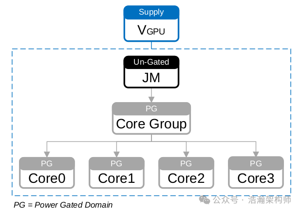
Figure 1-9 GPU Power Domains Example – Logical View
For the fine control of power domains within the GPU, the GPU Driver typically requires deep involvement. The driver makes decisions based on the system states (such as temperature, current GPU computational demand, CPU or memory load states) collected from OSPM to control the power domains within the GPU.
(2) Power domain control is often explained from a logical view, but there are differences between the physical view and logical view. The physical view corresponding to the logical view in Figure 1-8 is shown in Figure 1-10; please pay attention to the distinction.
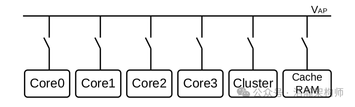
Figure 1-10 Processor Power Domains Example – Physical View
1.3.3 Example of Power Domain
Let’s look at an example of a power domain, as shown in Figure 1-11:
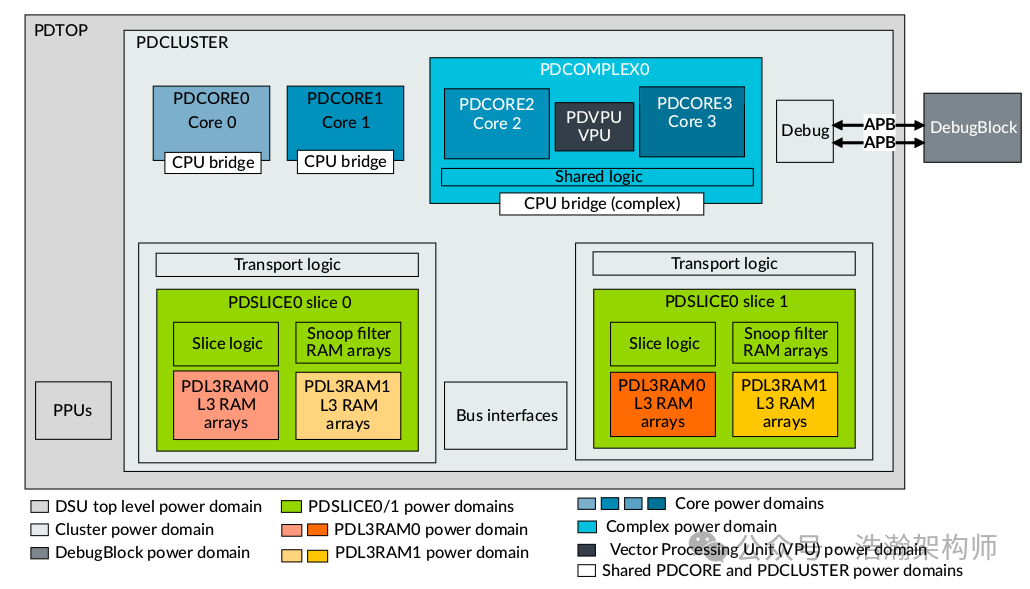
Figure 1-11 DSU-110 Power Domains
Let’s look at the description in the manual:
The DynamIQ ™ Shared Unit-110 (DSU-110) supports different power domains. You do not need to implement all power domains. The number and type of domains that are implemented depend on the choices made by the System on Chip (SoC) implementer. Each of the L3 cache slices, cores, and complexes can be placed in their own separate power domain. As the number of these components can vary depending on implementation, therefore the total number of power domains can also vary.
Although the DSU has many power domains, not all of them must be implemented; it is sufficient to meet the requirements. We will not elaborate on this section; future articles will continue to analyze power domain-related knowledge.
1.4 Logical Relationship Between Voltage Domains and Power Domains
Let’s briefly analyze the logical relationship between voltage domains and power domains through a view, as shown in Figure 1-12:
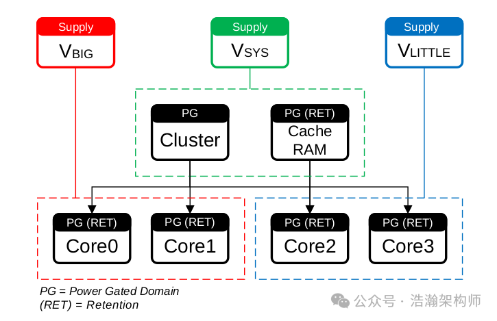
Figure 1-12 Processor Power Domains Example Logical View
From the above diagram, we can summarize the following:
(1) Power domains are a further subdivision of voltage domains. Voltage domains and power domains are two handles of PSCA power management, representing “micro” and “macro” means:
• The adjustment method of voltage domains, DVFS, can finely tune power consumption and performance, with a quick response time and immediate effect.
• The adjustment method of power domains involves switching power states, which is somewhat cumbersome and has a relatively longer response time.
(2) The operations of the two are not isolated but rather collaborative:
• The state adjustment of power domains is based on the voltage and frequency adjustments of voltage domains.
• The Always-On domain provides an anchor for waking up and also controls the layered power adjustments of voltage domains, ultimately fulfilling the functions of power domains.
(3) Software and hardware collaboration
• Both voltage domains and power domains rely on OSPM to maximize the energy efficiency of a SoC product, such as the Power management subsystem of the Linux kernel.
• Software management requires underlying SCP to provide mechanisms, which expose interfaces to the upper-layer OSPM power management module through frameworks like SCMI, ACPI, PSCI, etc.
We will gradually discuss these topics in future articles. Those who are eager can refer to relevant manuals and source codes.
Conclusion
By comparing with household circuits, we introduced the concepts of circuit area division and power operational states in power management. Based on this, we progressively displayed the system’s division into different voltage domains, and on the basis of voltage domains, further divided them into different power domains, providing examples of both voltage and power domains, and finally demonstrating the logical relationship between the two. This introduction lays the foundation for further discussions on power management under the ARM architecture. That’s all for today; please follow, comment, and share. Thank you all.
Reference
[01] <DEN0050D_Power_Control_System_Architecture.pdf>
[02] <armv8_a_power_management_100960_0100_en.pdf>
[03] <Power_Policy_Unit_Architecture_Specification.pdf>
[04] <DEN0024A_v8_architecture_PG.pdf>
[05] <79-LX-LD-s003-Linux设备驱动开发详解4_0内核-3rd.pdf>
[06] <80-PGxxx-35_QNX_Thermal_Manager_Overview.pdf>
[07] <80-pgxxx-7_n_qnx_power_management_software_architecture_ref.pdf>
[08] <80-ARM-POWER-HK0001_一文搞懂ARM_SoC功耗控制架构.pdf>
[09] <Arm_Power_and_Performance_Management_SCMI_White_Paper.pdf>
[10] <80-ARM-POWER-cs0001_Arm-SoC-power功耗控制架构.pdf>
[11] <80-LX-LK-cl0009_深入理解Linux电源管理.pdf>
[12] <DEN0056D_System_Control_and_Management_Interface_v3_1.pdf>
[13] <arm_total_compute_2021_reference_design_software_developer_guide_en.pdf>
[14] <arm_total_compute_2022_reference_design_software_developer_guide_en.pdf>
[15] <arm_cortex_m85_processor_trm_en.pdf>
[16] <DEN0108_00eac0_smcf-Architecture-Specification.pdf>
[17] <DEN0022F.b_Power_State_Coordination_Interface.pdf>
[18] <MTxxxx_SCP_User_Manual_V1.0.pdf>
[19] <learn_the_architecture_arm_system_architectures_en.pdf>
[20] <arm_dsu_110_trm_101381_0400_11_en.pdf>
Glossary
AP – application processor
OSPM – Operating System Power Management
WFI – Wait For Interrupt
WFE – Wait For Event
DVFS – Dynamic Voltage and Frequency Scaling
SCU – Snoop Control Unit
OPP – Operating Performance Point
PSCI – Power State Coordination Interface
PPU – Power Policy Unit
PCSA – Power Control System Architecture
SoC – System-on-Chip
PCF – Power Control Framework
SCP – System Control Processor
BSP – board support package
SCMI – System Control and Management Interface
EAS – Energy Aware Scheduling
IPA – Intelligent Power Allocation
ACPI – Advanced Configuration and Power Interface
LPI – Low-Power Idle
CPPC – Collaborative Processor Performance Control
PCSM – power control state machine
AOSS – Always-on subsystem
PMIC – Power Management Integrated Circuit
JM – job manager
AON – always on domain
SBSA – Server Base System Architecture
CLK_CTRL – Clock Controller
LPD – Low Power Distributor
LPC – Low Power Combiner
P2Q – P-Channel to Q-Channel Convertor
GPIO – General Purpose IO
RAS – Reliability, Availability, and Serviceability
STR – Suspend to RAM