
NVIDIA launched its new generation autonomous driving SoC, Atlan, after a year and a half of silence following the release of Orin in December 2019. The naming convention indicates that NVIDIA continues to use names from the “Aquaman” series. The Orin SoC announced by NVIDIA in 2019 was named after the first ruler of Atlantis. Today, NVIDIA announced the Atlan SoC, named after the father of Orin. Compared to Orin, Atlan is revolutionary; it is not merely a vehicle chip but rather resembles a large data center server chip, with less concern for cost and power consumption.
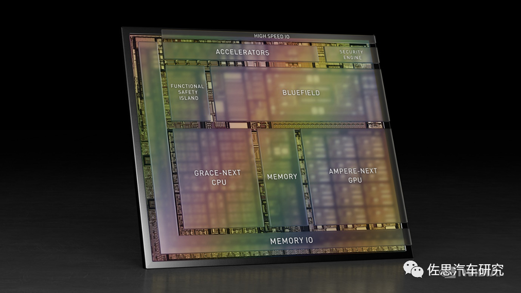
NVIDIA has never publicly disclosed the internal layout of the Orin chip, but Atlan’s layout was revealed from the start, perhaps indicating greater confidence in Atlan.
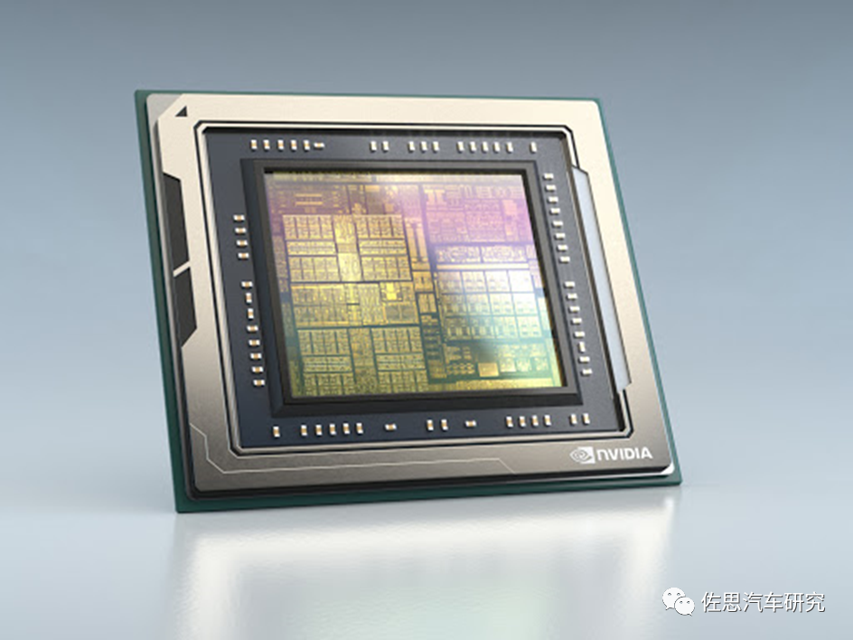
This is the official image of the Orin chip released by NVIDIA in November 2019. However, a rough layout of Orin can be found online.
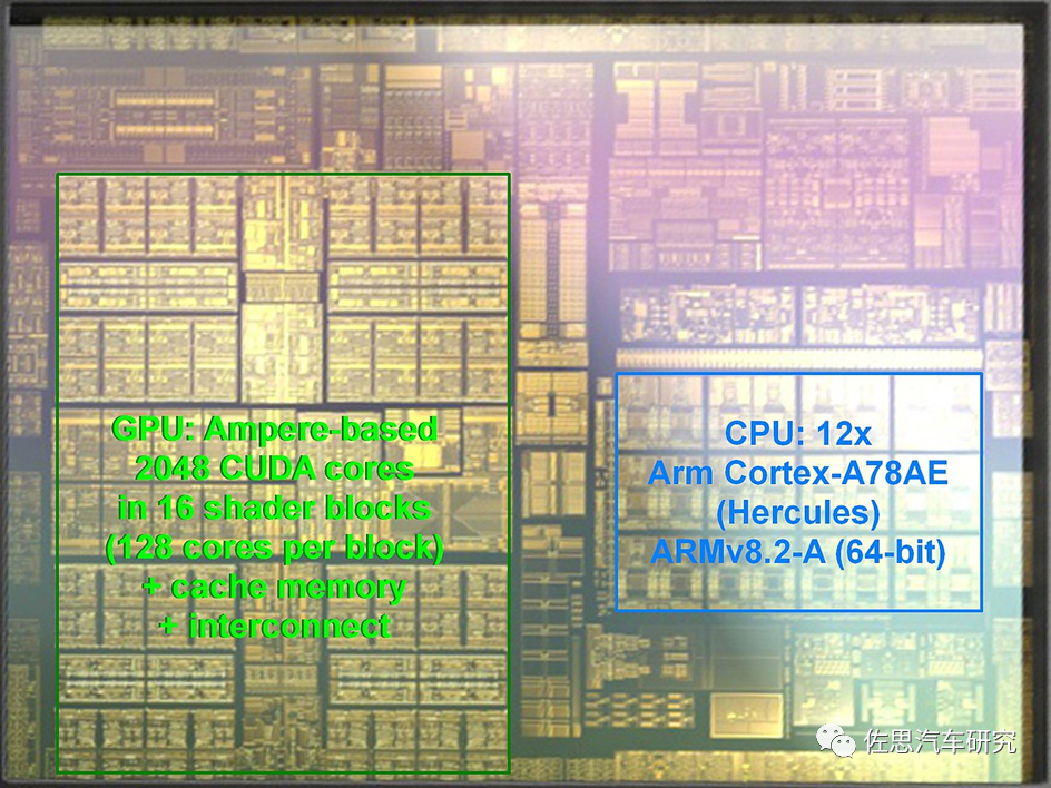
Source: https://en.wikipedia.org/wiki/Tegra#Orin
Atlan no longer uses the ARMv8 instruction set that has been in use for nearly a decade, instead opting for the ARM Neoverse V1 instruction set. Developers may need to invest significant effort to familiarize themselves with this previously unseen instruction set. The most significant change is that the CPU utilizes ARM’s Zeus architecture designed for the server domain, adding the Bluefield DPU component and incorporating a safety island design for functional safety. First, let’s look at the CPU section.
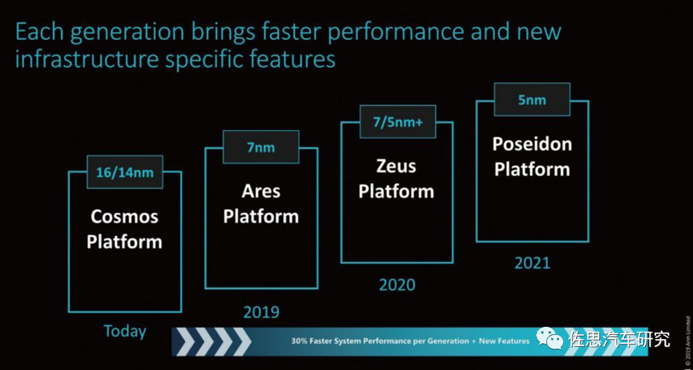
In March 2019, ARM launched the Neoverse platform targeting the server market, initially named Ares, after the Greek god of war; in 2020, it was Zeus, the highest god among the second generation of Greek gods; and in 2021, it was Poseidon, the Greek god of the sea. Perhaps there will be no Hades, the god of the underworld. At least this series can be referred to as the 11th generation.
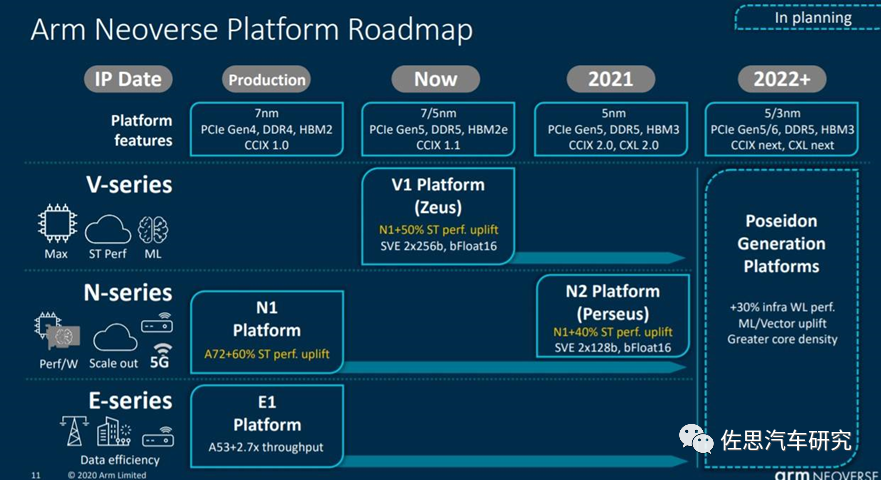
The Neoverse platform is further divided into three series: V, N, and E, corresponding to high performance, high efficiency, and low power consumption applications. The first product in the V series, by the way, is the N2 platform, codenamed Perseus, after the Greek hero who beheaded Medusa. The CPU that NVIDIA has introduced is based on the Zeus platform.
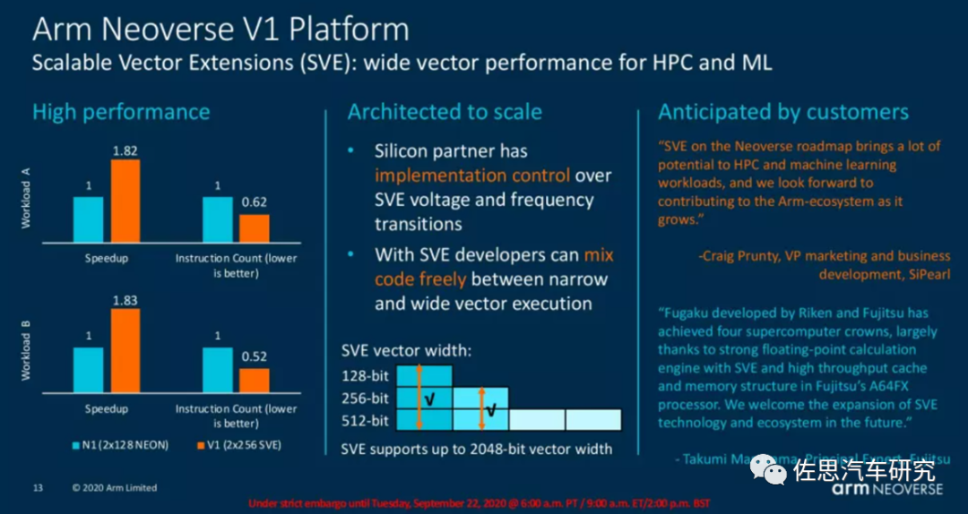
V1 can be seen as an enhanced version of the ARM v9 instruction set just released, with SVE (Scalable Vector Extension) being the most significant change. SVE is the next generation SIMD instruction set under the ARM AArch64 architecture, aimed at accelerating high-performance computing. The advanced SIMD (i.e., ARM NEON or “MPE” multimedia processing engine) instruction set of ARM v7 has been around for over a decade since its release in 2005. The main features of ARM v7 NEON are as follows:
-
Supports 8/16/32-bit integer operations, non-IEEE compliant single-precision floating-point operations, and conditional execution of instructions.
-
32 64-bit vector registers, which can also be viewed as 16 128-bit vector registers.
-
Aimed at accelerating multimedia processing tasks on the CPU side.
When upgrading to the ARMv8 architecture, the AArch64 NEON instruction set underwent many improvements, such as:
-
Support for IEEE compliant single-precision and double-precision floating-point operations and 64-bit integer vector operations.
-
2 128-bit vector registers.
-
These improvements make the NEON instruction set more suitable for general computing, not just multimedia computing.
However, the new market for ARMv8 requires more thorough improvements to the SIMD instruction set. There is a need to process unconventional data and complex data structures in parallel, as well as longer vectors, which led to the creation of SVE, aimed at accelerating high-performance computing.
- 128-bit multiples, supporting up to 2048 bits.
- Different implementations can adapt to various application scenarios without changing the instruction set.
- Per-channel prediction.
- Support for complex nested loops and if/then/else conditional jumps, without loop tail.
- Gather load and scatter store support for complex data structures, such as strided data access, array indexing, linked lists, etc.
- Horizontal operations.
-
Support for basic reduction operations, reducing loop dependencies.
SVE2 was released in April 2019 alongside V1, and the advantages of SVE and SVE2 lie in their variable vector sizes, ranging from 128b to 2048b, allowing for variable granularity of 128b vectors, regardless of the actual hardware running. From the perspective of vector processing and programming, this means that software developers will only need to compile their code once, and if a future CPU has a native 512b SIMD execution pipeline, that code will be able to fully utilize the entire width of the unit.
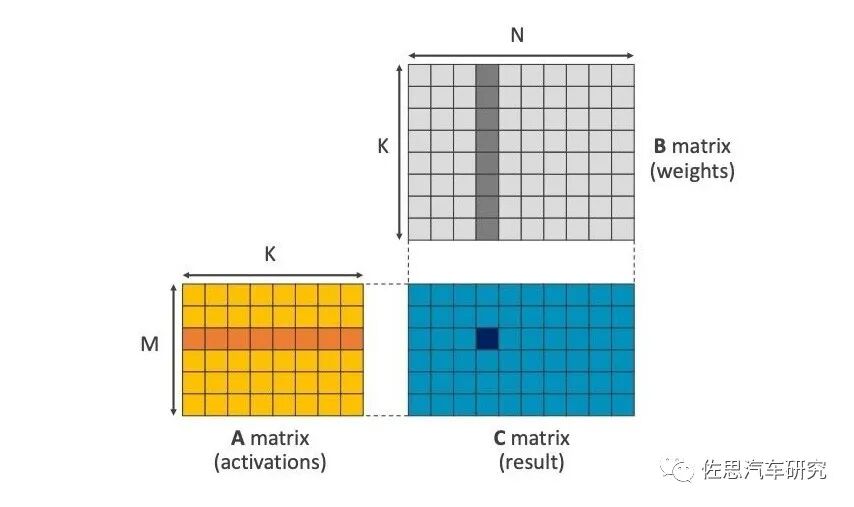
SVE2 is designed for machine learning, with the general matrix multiplication (GEMM) instruction being its most prominent feature. We all know that AI accelerators are essentially a stack of multiply-accumulate (MAC) operations, which can execute both multiplication and addition instructions at once. In essence, it is a matrix multiplication accumulator, and the GEMM instruction was also added in ARM v8.6. In the multiplication accumulator, multiplication must traverse each value in the matrix (usually pixels), which is the most time-consuming part, while the adder is much faster. ARM’s CPUs cannot stack MACs like AI can, but they can accelerate matrix multiplication, significantly reducing the workload on the backend multi-core processors. This is akin to a high-speed DSP, with a lower frequency but high bandwidth.
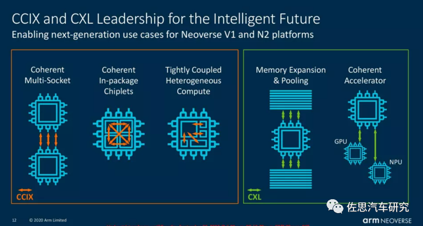
Another prominent feature of V1 is CCIX and CXL, which are the well-known chiplet concepts. The concept of chiplets is quite simple: it is die-level reuse. Designing a system-on-chip (SoC) used to involve purchasing various IPs from different suppliers, either soft cores (code) or hard cores (layouts), combining them with self-developed modules, and integrating them into a single SoC, completing the entire chip design and production process at a specific chip process node. In the future, for certain IPs, you may not need to design and produce them yourself; you can simply buy pre-implemented die and integrate them into a single package, similar to a System in Package (SiP), but there are significant differences between the two. Chiplets are wafer-level, mid-end packaging manufactured only by foundries, while SiP is chip-level packaging, which is the domain of specialized packaging manufacturers, involving ball-level packaging. Chiplets are also known as Multi-Chip Modules (MCM). In 2017, NVIDIA, the University of Texas, Arizona State University, the Barcelona Supercomputing Center, and the Polytechnic University of Catalonia jointly published a research paper titled “MCM-GPU: Multi-Chip-Module GPUs for Continued Performance Scalability,” which provides detailed research on this topic and was presented at the ISCA conference in Toronto, Canada, in 2017.
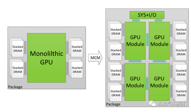
In simple terms, it means combining four small chips into one large chip, which NVIDIA refers to as MCM technology.
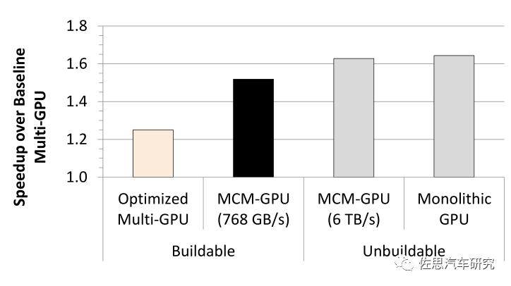
The above image compares the performance of NVIDIA’s MCM-GPU with multiple GPUs. NVIDIA proposed the RC-18 concept at the 2019 VLSI conference, utilizing 36 small chips.
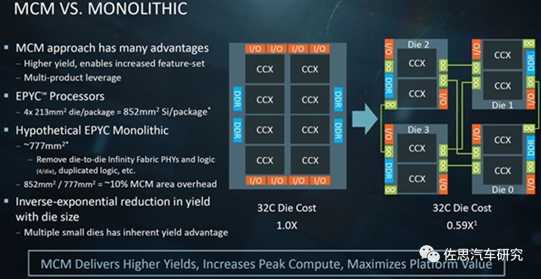
Not only GPUs or AI chips can do this; CPUs can as well. This is the key to AMD’s rise in the server domain, with the most typical example being AMD’s 32-core (which should be 32 small chips) EPYC. The biggest advantage of this approach is cost; if packaging 32 cores into a single chip costs 1, their MCM approach only costs 0.59, saving 41% in costs.
Combining small chips into a large chip may seem like a “glue” method, but the actual threshold is very high. Only TSMC’s CoWos and Intel’s EMIB processes can support this. NVIDIA has traditionally preferred Samsung over TSMC, as they know that over-reliance on TSMC can lead to supply chain issues, which is why NVIDIA has largely abandoned the MCM route.
Returning to Atlan, it is possible that Atlan uses the CXL chiplets provided by ARM V1 for memory expansion, as reducing the physical distance between memory and processors is the most effective way to address the memory bottleneck in AI processors. CCIX is more complex and may be used in the next generation.
Next, let’s look at the Bluefield DPU section. In April 2020, NVIDIA spent $7 billion to acquire the Israeli chip company Mellanox Technologies, Ltd., and by integrating Mellanox’s technology, the new NVIDIA will possess end-to-end technology from AI computing to networking, as well as a full-stack product from processors to software, with sufficient scale to advance the next generation of data center technology.
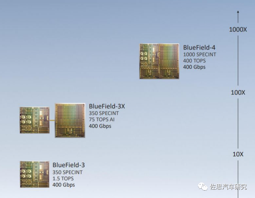
Mellanox’s main product is the Bluefield chip, which NVIDIA has renamed to DPU. It is essentially an advanced network card. The DPU is specifically designed to handle tasks that would typically require CPU processing, such as networking, storage, and security. This means that if a DPU is used in a data center, much of the CPU’s computational power can be freed up. According to NVIDIA, one DPU has the network processing capability equivalent to 125 CPUs.
NVIDIA plans to launch the third generation of Bluefield in 2022. In more complex terms, a DPU is a programmable electronic component that processes data streams, with data being transmitted as reusable packets and components. The DPU possesses the generality and programmability of a CPU but is specialized for efficiently processing network data packets, storage requests, or analysis requests. The DPU excels over CPUs due to its greater parallelism (capable of processing more data simultaneously).
At the same time, the MIMD architecture of the DPU is superior to the SIMD architecture of GPUs, as each request requires different decisions and follows different paths through the chip, distinguishing it from GPUs. This is what NVIDIA refers to as software-defined networking. Mellanox’s NVMe SNAP (software-defined network acceleration processing) technology can provide 2.5M + IOPS read/write access for remote storage, achieving line-speed performance of 100Gb/s with a block size of 4KB. In contrast, entry-level NVMe SSDs can provide 300K IOPS with 4KB blocks. Additionally, the BlueField-2 DPU effortlessly adds IPSec encryption and decryption capabilities at 100 Gb/s.

The above image shows the second generation Bluefield, which contains 8 ARM A72 cores. The data bandwidth to be processed in Atlan is far less than that of traditional servers, and two A72 cores are sufficient. The DPU in Atlan is primarily aimed at the vehicle backbone Ethernet and external PCIe networks, with built-in network controllers and PCIe switches. Ethernet can easily support up to 100G, while PCIe supports up to the fourth generation, and it can also serve as a network interface chip for data collection vehicles, connecting to ultra-high-speed solid-state drives. However, the physical layer chips still rely on Marvell, Texas Instruments, and Broadcom.
Finally, there is the functional safety isolation island, which should be the Cortex-R52 released by ARM. The functional safety island mentioned by NVIDIA is essentially consistent with ARM’s promotional terms for safety islands. The R series is ARM’s core specifically developed for high real-time requirements, with the R52 being the flagship product of the R series. NVIDIA’s chips have never used R cores before.
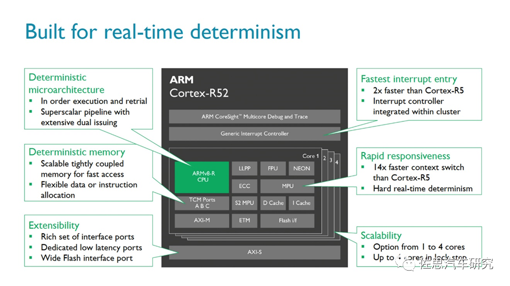
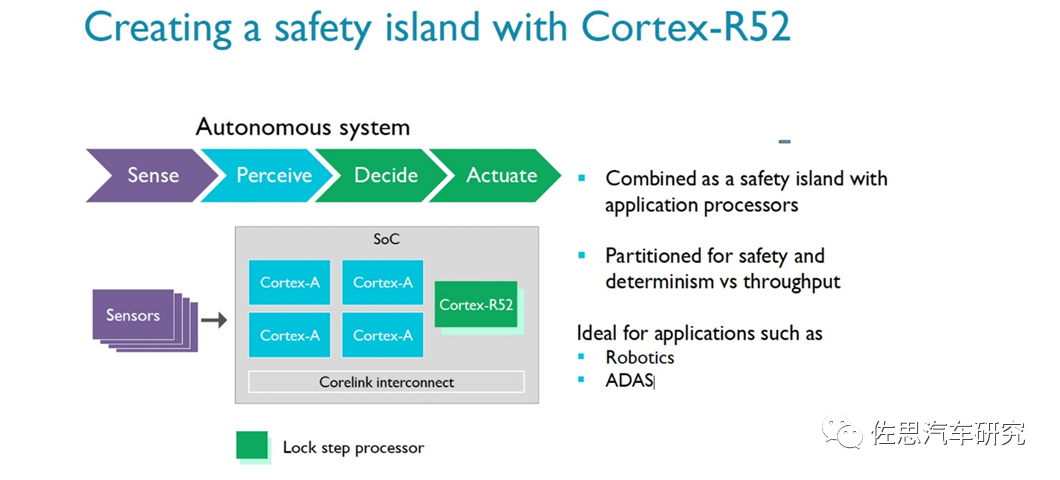 The R52 is a core specifically designed for the autonomous driving safety market, released by ARM in 2016. The Cortex-R52 supports up to 4-core lockstep technology, offering a 35% performance improvement over the Cortex-R5, with a 14-fold increase in context switching (out-of-order) and a 2-fold increase in entry preemption, supporting hardware virtualization technology. According to ARM, a simple central control system can directly use the Cortex-R52, but for applications like industrial robots and ADAS (Advanced Driver Assistance Systems), it is recommended to pair it with Cortex-A, Mali GPU, etc., to enhance overall computation. Additionally, the ARM Cortex-R52 has passed multiple safety standard certifications, including IEC 61508 (industrial), ISO 26262 (automotive), IEC60601 (medical), EN 50129 (automotive), and RTCA DO-254 (industrial). In March 2021, the R52+ architecture was also launched, supporting up to 8-core lockstep. The R52 includes three major functions: software isolation, which is achieved through hardware, meaning that software functions do not interfere with each other. For safety-related tasks, this also means that less certified code is required, saving time, costs, and workload.
- Support for multiple operating systems: With virtualization capabilities, developers can use multiple operating systems within a single CPU to integrate applications. This simplifies the addition of functionalities without increasing the number of electronic control units.
-
Real-time performance: The high-performance multi-core cluster of Cortex-R52+ can provide real-time response capabilities for deterministic systems, with the lowest latency among all Cortex-R products.
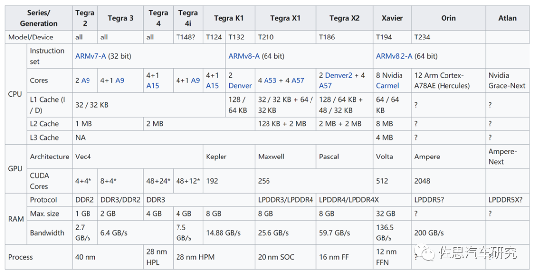
Atlan boasts up to 1000 TOPS of computing power, which is four times that of Orin. Looking at its internal layout, it still features 12 Ampere GPU modules, similar in area to Orin, perhaps even slightly smaller. However, the die area of Atlan’s CPU is significantly larger than that of Orin. The achievement of 1000 TOPS in Atlan is primarily attributed to the CPU, DPU, and storage, as the improvements in the Ampere architecture alone are unlikely to account for such a significant increase. Atlan is designed for ultra-large-scale models in servers,while the trend for autonomous driving vehicle models is towards smaller sizes and lower precision, with some even calling for 1-bit precision. Atlan goes against this trend, particularly supporting BFloat16 precision, which is common in server domains but rare in autonomous driving. Clearly, Intel’s interest in the automotive sector is gradually declining, as both the CPU and DPU are derived from the server domain rather than being specifically developed for automotive applications. In the ARM server domain, leveraging deep cooperation with ARM and a solid technical foundation, NVIDIA can update its products every two years like Intel’s laptops. However, the lifecycle of a vehicle is at least 7-8 years, and car manufacturers are unlikely to agree to such an update frequency.However, NVIDIA does not mind; its core business remains graphics cards and data center processors, with automotive being a secondary focus, utilizing the residual capabilities of CPU, GPU, and DPU. While Orin’s ARM A78 core was introduced specifically for autonomous driving, it is not seen in NVIDIA’s other products, highlighting the importance placed on the A78, whereas Atlan reflects a focus on data centers.NVIDIA’s other intention is to engage competitors in a computing power arms race, creating a significant promotional push to pressure competitors to follow suit in the computing power game until they are overwhelmed. Other manufacturers are unlikely to follow this computing power number game, as it deviates from actual demand. Orin is likely to be NVIDIA’s main product for the coming years.
Research Report Writing Plan by Zosi 2021
Panorama of the Intelligent Connected Vehicle Industry Chain (March 2021 Edition)
2021 Zosi Automotive Conference Activity Plan
「Zosi Research Annual Report and Quarterly Report」
|
OEM Autonomous Driving |
Low-speed Autonomous Driving | Automotive Vision (Upper) |
| Automotive Vision (Lower) | Commercial Vehicle Autonomous Driving | Emerging Vehicle Manufacturing |
| Automotive MLCC | Automotive Car Sharing | High-Precision Mapping |
| Automotive Simulation (Upper) |
Automotive Simulation (Lower) |
Automotive and Domain Controllers |
| APA and AVP | Vehicle Laser Radar | Millimeter Wave Radar |
| Processor and Computing Chips | ADAS and Autonomous Driving Tier 1 | Passenger Vehicle Camera Quarterly Report |
| HUD Industry Research | Driver Monitoring | Automotive Power Semiconductors |
| Radar Disassembly | OEM Vehicle Networking | T-Box Market Research |
| Automotive Gateway | In-Vehicle Voice | Automotive Wiring Harness and Cables |
| Automotive Intelligent Cockpit | Human-Machine Interaction | V2X and Vehicle-Road Collaboration |
| Automotive Operating Systems | L4 Autonomous Driving | Dedicated Vehicle Autonomous Driving |
| Computing Platforms and System Architectures | In-Vehicle Infrared Night Vision Systems | Shared Mobility and Autonomous Driving |
| High-Precision Positioning | Automotive OTA Industry | Automotive IGBT |
| Cockpit Multi-Screen and Linked Screens | Daimler’s New Four Modernizations | Tesla’s New Four Modernizations |
| Volkswagen’s New Four Modernizations | BYD’s New Four Modernizations | Intelligent Rearview Mirrors |
| Huawei’s New Four Modernizations | Four-Dimensional Map’s New Four Modernizations | Fuel Cells |
| AUTOSAR Software | Cockpit SOC | Steer-by-Wire Chassis |
| In-Vehicle Displays | Roadside Intelligent Perception | Autonomous Brand Vehicle Networking |
| Automotive Digital Keys | Automotive Cloud Service Platforms | Wireless Communication Modules |
| ADAS/AD Main Control Chips | Tier 1 Intelligent Cockpit (Upper) |
Waymo Intelligent Connected Layout
TSP Manufacturers and Products
「Zosi Research Monthly Report」
ADAS/Smart Vehicle Monthly Report | Automotive Cockpit Electronics Monthly Report | Automotive Vision and Radar Monthly Report | Battery, Motor, and Control Monthly Report | In-Vehicle Information System Monthly Report | Passenger Vehicle ACC Data Monthly Report | Front View Data Monthly Report | HUD Monthly Report | AEB Monthly Report | APA Data Monthly Report | LKS Data Monthly Report | Front Radar Data Monthly Report
Report Order Contact: Mr. Fu 15810027571 (WeChat available) Ms. Liao 13718845418 (WeChat available)