The design of the power grid has a direct impact on chip performance and reliability. It is essential to ensure that the power grid provides sufficient power voltage to all transistors within the cells, allowing the chip to operate normally under all possible conditions within a certain noise tolerance. However, as technology shrinks, the threshold voltage of transistors does not decrease as rapidly as the power voltage, leading to a significant reduction in the circuit’s tolerance to voltage drops. This results in a smaller logic noise margin, decreased chip performance, and even functional failures in integrated circuits.With the scaling of technology, designing power grids in large SoC designs with limited power becomes challenging. Static IR drop is calculated early in the design to estimate average voltage drops and provide some feedback in the initial power grid design. However, relying solely on static IR drop validation is insufficient to ensure power integrity, as it does not account for power density, switching activity, and the effects of inductance and decoupling capacitance. In particular, dynamic IR drop often has a significant impact on chip functionality, making it one of the primary criteria for chip tape-out approval.Dynamic Power and IR Drop CalculationDynamic power consists of internal power and switching power, as shown in the formula. Where internal power is consumed due to the charging and discharging of internal load capacitance, and switching power is consumed due to the charging and discharging of output load capacitance of the cells.The evaluation of dynamic IR drop is based on the peak current demand caused by standard cell switching, including decoupling capacitance, inductance, and spatial and temporal circuit switching. Non-vector IR drop uses current constraints early in the design to capture circuit uncertainties and assess the worst-case IR drop at each node in the power grid. In the case of vector IR drop, we can observe localized IR drop hotspots caused by high power scenarios.Next, various IR drop reduction techniques will be attempted. The first is a robust P/G track structure to reduce IR drop for all placed standard cells. The second is to add extra Power Switch Units (PSW) to fix localized IR drop hotspots. The third is P/G grid sharing to improve the IR drop performance of memory IPs. All experimental results are conducted using ANSYS RedHawk, the leading commercial EDA tool for IR drop sign-off.A. Robust P/G Track StructureThe use of power metal in the power grid (width, spacing, pitch, metal/via stacking, etc.) is defined by the module power specifications. If certain modules consume more power, we must use wider metal for the grid in this case. Due to the smaller width/thickness, the resistivity of lower metal layers increases. The power tracks are composed of the lowest metal layers to connect the P/G pins of standard cells, with smaller widths. Therefore, due to the higher track resistance, most of the current reduction occurs at the power tracks. If a module has lower current consumption, a single track is sufficient to ensure current flow.Figure 1 shows the proposed dual-track structure, which may be one of the good solutions to reduce IR drop for high power modules. The IR drop performance of the dual track is relatively equivalent to the expansion of metal width. As shown in Figure 2, in our design, applying dual tracks shows an improvement of about 3 percentage points compared to the previous single track structure.
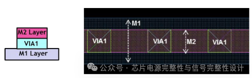 Figure 1. Dual-track metal stacking. Cross-section (left), top view (right).
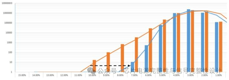 Figure 2. Dual-track structure improves IR drop performance.B. Adding Extra Power Switch Units in Local Hotspot AreasPower gating is a technique used in SoC design to reduce power consumption by cutting off power current to unused circuit modules. PSW units are used to implement power gating designs for power domains, and PSW is a special low-leakage PMOS transistor known as header-type PSW.The initial power grid should meet the IR drop budget without excessive design to prevent loss of additional routing resources. However, during dynamic IR drop analysis, some localized hotspots may occur due to high power scenarios, which are often unpredictable. Local hotspots typically appear in certain physical design modules (such as CPU/GPU cores) because these modules have recently reached operating frequencies above 2-3GHz. Therefore, there must be timing-critical areas in the design with high cell density, which become dynamic IR drop hotspots.When we fix the dynamic IR drop of localized hotspots, we first attempt to expand the cells and reroute signal interconnections within the timing margin. However, if the timing margin in that area is very small, this attempt will be a very time-consuming iterative process. In this case, adding extra PSW in localized hotspots may be the best solution to reduce IR drop values. It reduces the average resistance path required for current to reach standard cells. However, the additional PSW will increase small leakage power and must also consider area overhead. As shown in Figure 3, the IR drop hotspot (red area) is significantly reduced.
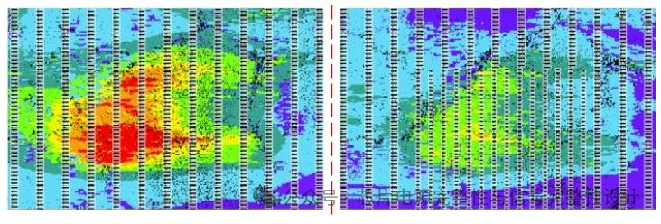 Figure 3. Fixing localized IR drop hotspots by adding extra PSW. Before (left) and after (right).C. Sharing Memory P/G GridsMany compiled memory IPs are used in SoC design, so appropriate layout planning should be considered to reduce area loss and timing issues. In this case, synchronizing P/G routing above the memory will be very difficult. If we rely on P&R tools to route the P/G grid, it will route across various memories.Since the memory has M4 P/G pins, metal layers 5 and 6 directly affect IR drop performance. If we adjust the memory positions to share M5 and M6 with adjacent memories, more current paths can be formed, which will greatly help improve the IR drop performance of the memory. As shown in Figure 4, in our design, the IR drop performance improved by 1.2 percentage points compared to the non-sharing scheme. In particular, we can see that the red area (highest IR drop area) in Memory A has been eliminated.
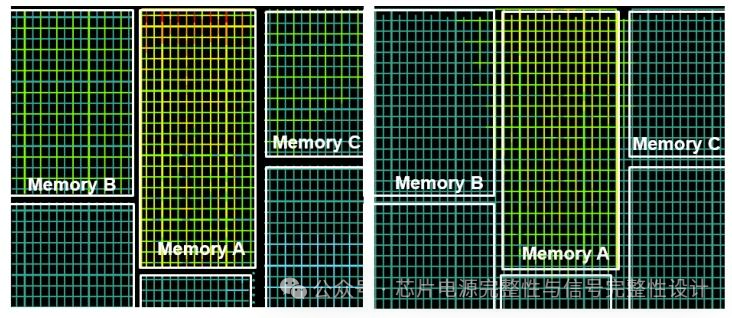 Figure 4. Sharing P/G grid with adjacent memory IPs. Before (left) and after (right).ConclusionFrom the results of various IR drop reduction techniques used in FinFET SoC design mentioned above, all can facilitate the sign-off of on-chip IR drop.