Hello everyone, this is Hardware Talk!
It has been a while since the last update. I wonder if everyone has been learning in the past few months? I believe many of you have! I apologize for not updating related content; it’s not that I didn’t want to, but I have been improving myself. I needed to enhance my skills first to summarize and extract more valuable insights for our collective progress.
Today, I would like to analyze the working principle of ADC.
1. Analog-to-Digital Conversion
Analog-to-digital conversion serves as a bridge for converting analog signals into digital signals. Analog signals are susceptible to interference, and their processing can be limited by various conditions, making them difficult to store. Therefore, in practical applications, they are often converted into digital signals. When outputting, they are converted back into analog signals, with a typical application being Class D amplifiers.
In an ADC signal chain, there are at least five components: front-end sensors, signal conditioning, anti-aliasing filtering, input protection, and the ADC itself. In the analog section, the ADC is the endpoint, while in the digital section, the ADC is the input, making it the core module that links analog and digital signals.
2. Working Principle of ADC
The ADC completes the transformation of analog signals into digital signals, and the devices that achieve ADC conversion mainly include the following four processes: sampling, holding, quantization, and encoding.
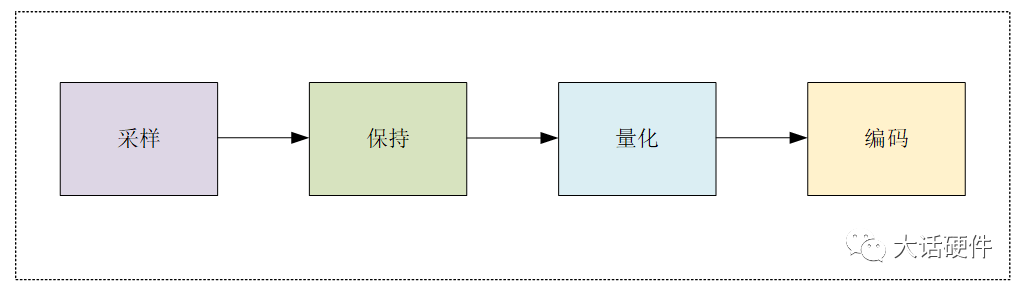 The corresponding circuit is shown below:
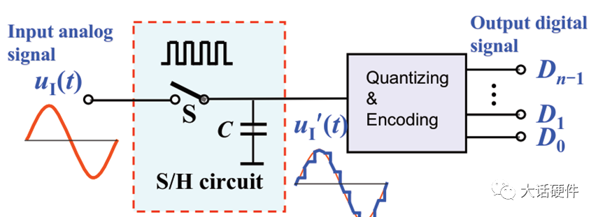
Currently, there are many types of ADCs on the market. If we delve into the internal details of ADCs, the sampling and holding circuits are fundamentally similar, but there are significant differences in quantization and encoding. It is precisely these differences that give rise to various ADC architectures such as SAR, pipeline, etc.
2.1 Sampling Theorem
Analog signals change continuously over time, while digital signals are discrete. To obtain the converted digital signal, the first step is to sample the analog signal. Since digital signals cannot be continuous over time, they can only sample the input signal at certain intervals. The number of samples taken per unit time is called the sampling rate, measured in Ksamples per second.
According to the Nyquist theorem, to reconstruct the sampled signal back into the input signal, the following condition must be met:
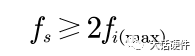
Where fs is the sampling frequency, and fimax is the frequency of the highest frequency component of the input analog signal. In practical circuit design, the sampling frequency is typically 3 to 5 times the maximum frequency.
During the sampling process, two theorems are often confused: the Nyquist sampling theorem and the Shannon sampling theorem, which is also known as the Nyquist-Shannon sampling theorem. Relevant materials can be consulted for further study.
2.2 S/H Holding Circuit
The core of the holding circuit is to maintain the sampled analog signal for a period of time, during which the signal must remain unchanged, allowing the subsequent digital circuit to complete quantization and encoding. Capacitors are typically used as the holding device after sampling. The principle is shown below:
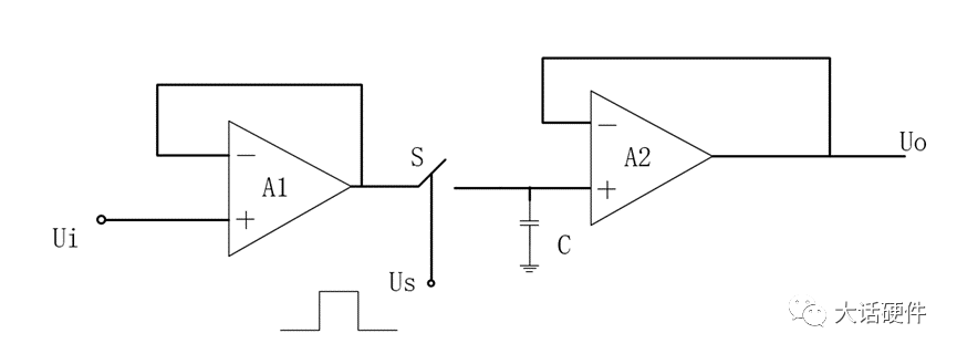
The capacitor C in the figure is the holding capacitor. The sampling switch and holding capacitor are usually combined as a single unit, referred to as the S/H circuit. A1 and A2 are two operational amplifiers configured as followers. These two operational amplifiers exist in the IC, with A1 used to isolate the preceding signal while utilizing the characteristic of infinite input resistance. A2 is used to isolate the subsequent signal, taking advantage of the output impedance of 20 to 50 ohms. With operational amplifiers on both sides, the S/H circuit is sandwiched in between, which can reduce noise.
Based on the principles of the sampling and holding circuits mentioned earlier, the first two processes can be simulated.
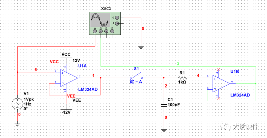
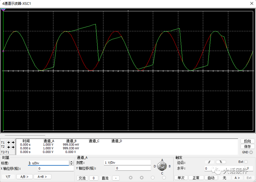
Assuming the sampling rate is relatively low, it can be manually satisfied. From the waveform below, the red line represents the original waveform, and the blue line represents the sampled signal, which shows significant distortion, indicating that the sampled signal cannot be accurately restored.
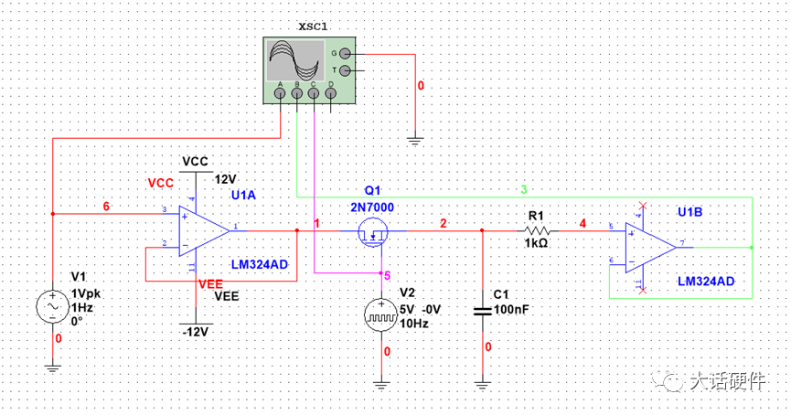
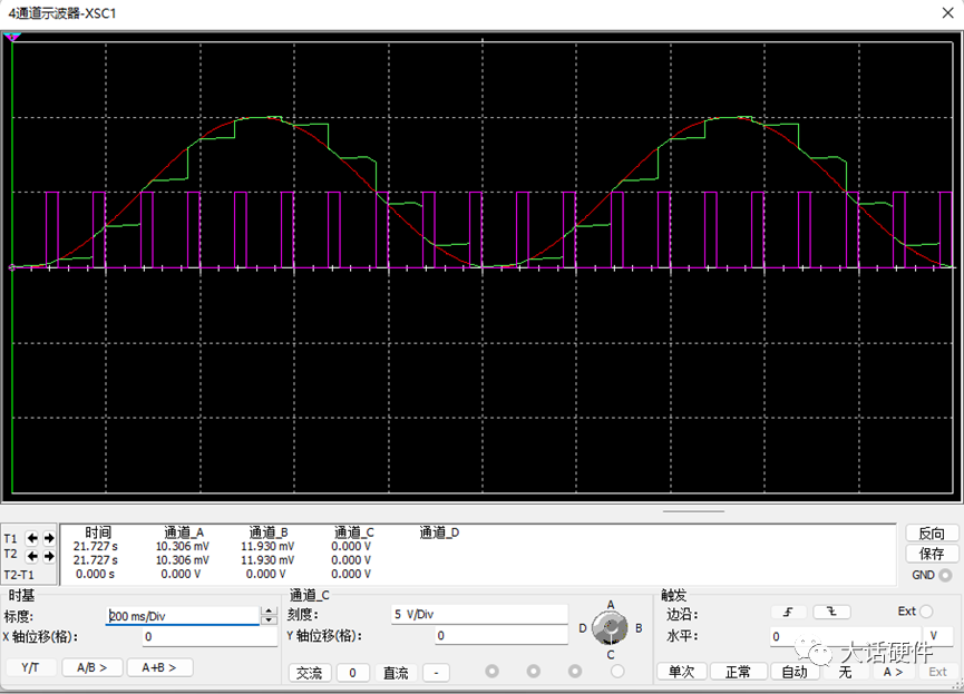
By replacing the switch with a MOSFET and adding the sampling drive frequency, the simulation results show that the red waveform is the input signal, and the blue is the sampled signal, which can basically restore the input signal.
2.3 Quantization
Quantization refers to approximating a continuous analog signal with a finite number of discrete digital signals. The quantized analog signal is divided into a finite set of equal amplitude steps, as shown in the figure below. 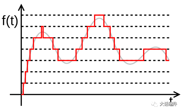
The original analog signal is continuous and infinite, while the digital signal used for quantization is discrete and finite. During the quantization process, due to the limited number of steps, some analog signals may be replaced by the same quantized value. As shown in the figure above, when the discrete digital signal takes a certain value, the corresponding analog signal is continuously changing. Therefore, there exists a difference between the original signal and the quantized signal, known as quantization error.
According to the definition of quantization error, if we were to use an infinite number of discrete values to quantize the analog signal, each step would be a point, and it would be almost identical to the original signal, resulting in no quantization error. However, this is not practically possible, so the fundamental reason for the existence of quantization error is the limited resolution used during quantization.
Resolution and accuracy are often confused. In middle school physics, we learned that resolution describes the scale division, while accuracy describes the degree of correctness. For example, if we have two rulers, both 10 cm long, one has 100 small divisions, and the other has 10 divisions, the former has a resolution of 1 mm, while the latter has a resolution of 1 cm. Clearly, the former has a higher resolution than the latter. In ADCs, the scale division is represented by the number of bits in the digital signal; for instance, an ideal 8-bit ADC has lower resolution than an 18-bit ADC.
Accuracy indicates the error between the measured value and the true value, or the extent to which the measured value deviates from the true value. Using two identical resolution ADCs to measure the same analog quantity will not yield identical results. Ignoring quantization error, the ADC itself will deviate from the true value due to the influence of device materials and manufacturing processes. To describe the magnitude of this accuracy, absolute accuracy and relative accuracy are commonly used. Absolute accuracy is expressed as a multiple of voltage resolution (LSB), such as ± 1/1LSB, ± 1LSB, etc. Relative accuracy is expressed as a percentage of absolute accuracy divided by the full-scale value.
The differences in quantization encoding lead to different types of ADCs.
2.4 Encoding
Encoding is the final process of internal conversion in the ADC, where the quantized results are represented in binary or other numeral systems, which is the encoding process. After encoding, the original analog signal becomes a digital signal. The essence of encoding is to output a string of numerical codes that closely approximate the currently sampled analog value. Therefore, the method of quantization will determine the rules of encoding.
Now, consider a 3-bit ADC quantizing and encoding an input voltage of 0 to 1V, the process is as follows.
A 3-bit ADC can quantize the input signal into 8 equal steps.
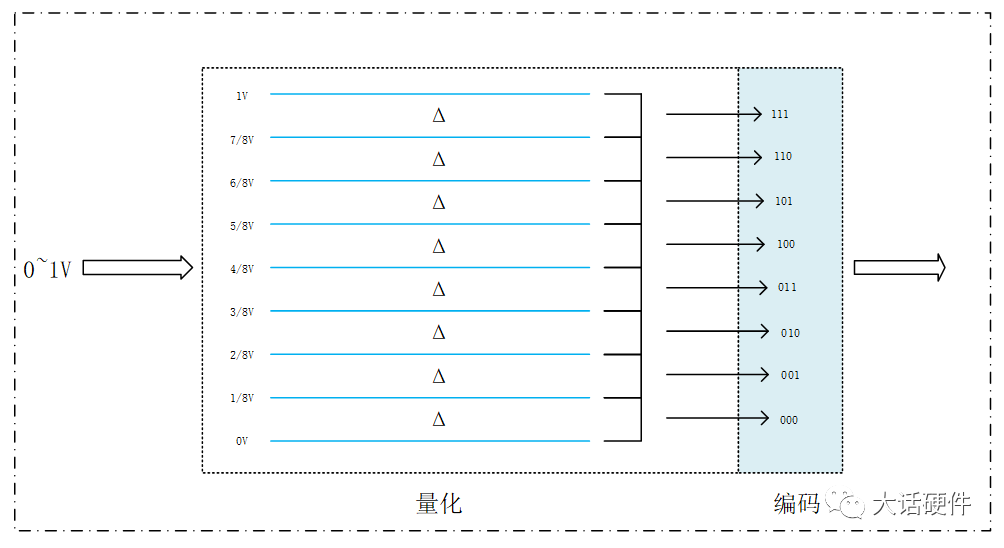
From the quantization process, it can be seen that when the input voltage is between 0 and 1/8V, the output code is 000 for any analog value. When the input voltage is between 1/8 and 2/8V, the output code is 001. Thus, the maximum quantization error introduced by this quantization process is 1/8V, which is the value of one step, or 1LSB. As the resolution increases, the analog quantity can be quantized into more bits, thereby reducing quantization error.
With the development of digital circuits, ADCs are actually used less frequently by most people, not because ADCs are no longer needed, but because upstream chip companies have integrated ADCs into their chips, directly outputting digital signals. However, whether in a separate signal chain or integrated within a chip, the overall framework of ADCs remains unchanged.

Follow me, and let me be your exclusive little sunshine!