The BJT amplifier circuit requires distortion-free amplification of small signals, with a larger voltage gain Au being preferable, a wider bandwidth being better, and a larger AC input resistance Ri being desirable, while a smaller AC output resistance is also preferable.
In the Multisim workspace, place 1 DC power supply V1 (12V), 1 AC small signal source V2 (effective value 5mV, frequency 1kHz), 1 resistor R2 (1k Ω, simulating V2‘s internal resistance), 1 resistor R1 (500k Ω), 1 resistor R3 (3k Ω), 1 resistor R4 (10k Ω, load resistor), 1 BJT Q1 (2N2221), 2 polarized capacitors C1 and C2 (both 10uF), connect as shown in the figure below. Since the BJT base is connected to a fixed resistor R1, the small signal is coupled to the amplifier circuit through capacitor C1, and the amplifier circuit is coupled to the load R4 through capacitor C2, this circuit is referred to as a capacitive coupled fixed bias common emitter amplifier circuit.
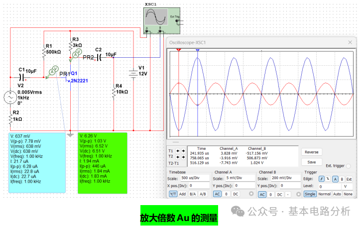
(1) Measurement of the amplification factor Au. Use probe PR1 to measure the BJT base potential and current, probe PR2 to measure the BJT collector potential and current. Channel A of the dual-trace oscilloscope observes V2 and the input small signal after being in series with R2, while channel B observes the output voltage waveform across R4. Start the simulation, the base DC potential is 637mV, the collector DC potential is 6.26V, and the BJT operates in the amplification state. The BJT AC current amplification factor β is 446/6.28 ≈ 71, rbe=300+[(71+1)×26/1.83] ≈ 1.3k Ω, the distortion-free amplification factor of this circuit Au=- β×(R3//R4)/rbe ≈-127. From the oscilloscope waveform, the output waveform is undistorted, and at time T2 the output voltage is 506.873mV, the input voltage is-3.916mV, the amplification factor is 506.873/-3.916 ≈-129, converting to decibels 20lg129 ≈ 42.21dB, which is not far from the theoretical estimate.
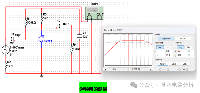
(2) Measurement of the bandwidth. Remove the two probes and oscilloscope, place 1 Bode plotter XBP1, connect the input terminal IN to the positive of V2 and ground, and connect the output terminal OUT to both ends of R4. Start the simulation, the Bode plotter displays the following figure. The position of the indicator line at 1kHz corresponds to an amplification factor of 42.462dB, which is basically consistent with the theoretical estimate. Moving the indicator line, the low-frequency cutoff frequency is approximately 12Hz, and the high-frequency cutoff frequency is approximately 11.53MHz, making the bandwidth of this circuit approximately 11.5MHz.
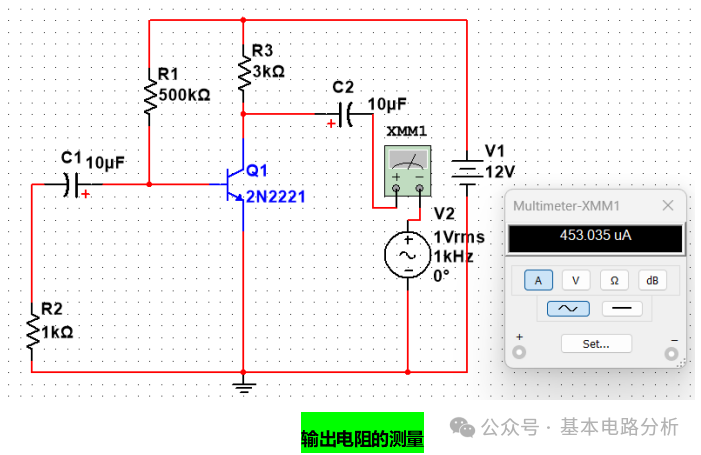
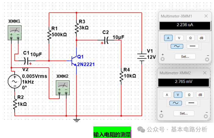
(3) Measurement of the input resistance Ri. The input resistance is defined as the ratio of the input port voltage to the input port current in the AC path. Theoretical analysis shows that the input resistance of this circuit is Ri=R1//rbe=500//1.3 ≈ 1.29k Ω. Insert the multimeter XMM1 in series with the branch where V2 is located to measure the AC current at the port; the multimeter XMM2 measures the AC voltage at the port after V2 is in series with R2, the measurement results are shown in the figure below. It can be seen that Ri=2.765/0.002236 ≈ 1.24k Ω, which is not far from the theoretical estimate.
(4) Measurement of the output resistance Ro. The output resistance of the amplifier circuit is defined as the ratio of the AC voltage to the port current when the input small signal is shorted, and the load is open. Theoretical analysis shows that the output resistance of the fixed bias common emitter amplifier circuit Ro ≈ R3 ≈ 3 k Ω. Short circuit V2, open R4, and apply an AC voltage source V2 (effective value 1V, frequency 1kHz) at the original position of R4, the multimeter XMM1 measures the current through the branch of V2. Start the simulation and find that the multimeter reading is 453.035uA, thus the output resistance of this amplifier circuit Ro=1/0.453 ≈ 2.21k Ω, which is not far from the theoretical estimate.