
In the field of semiconductor packaging, bonding strength is a key indicator for assessing packaging reliability. The editor of Kezhun Measurement and Control has specially compiled industry standard testing methods to help engineers accurately evaluate the quality of gold wire bonding, chip mounting, and other processes.
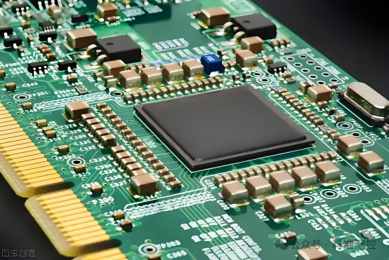
This article will detail the three main types of bonding strength tests: gold wire tensile testing, gold ball push testing, and chip push testing, covering core content such as testing principles, execution standards, instrument selection, and operational processes, providing standardized guidance for semiconductor packaging process validation.
Analysis as follows

1. Testing Principles

The bonding strength test evaluates the reliability of various connection points in semiconductor packaging by simulating mechanical stress, mainly including three testing modes:
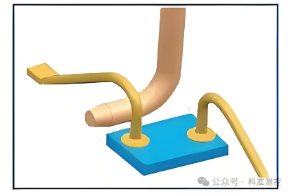
1. Gold wire tensile testing: Evaluates the bonding strength between the wire and the solder joint by vertically pulling the bonding wire with a hook needle.
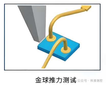
2. Gold ball push testing: Evaluates the bonding quality between the solder ball and the substrate using horizontal push force.
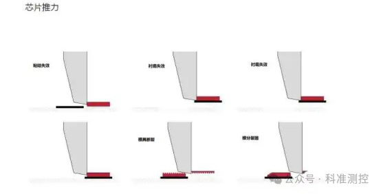
3. Chip push testing: Measures the mounting strength between the chip and the substrate.
These tests can effectively identify issues such as poor soldering and defects in the metallization layer, ensuring the reliability of the packaging structure during subsequent processing and use.
2. Testing Standards
1. Gold wire tensile testing standards
Testing specifications:
Hook needle position: Highest point of the gold wire arc
Testing speed: 0.2-0.5mm/s
Environmental conditions: 23±5℃, RH 45±15%
Fracture mode determination:
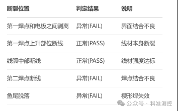
Tensile standard value (referencing MIL-STD-883G):
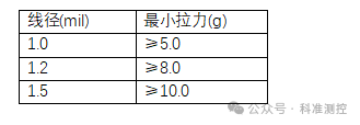
2. Gold ball push testing standards
Testing specifications:
Push knife height: 1/3-1/2 of the solder ball height
Contact angle: 90±5°
Testing speed: 50-200μm/s
Failure mode determination:
TYPE 1: Complete peeling of the gold ball (PASS)
TYPE 2: Peeling of the gold ball with slight metal residue (PASS)
TYPE 3: Substrate pit (FAIL)
TYPE 4: Push knife contacts the chip surface (FAIL)
TYPE 5: Partial peeling of the gold ball (FAIL)
TYPE 6: Metal layer detachment (FAIL)
Push standard value:
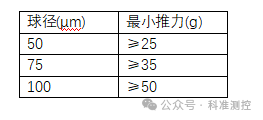
3. Chip push testing standards
Testing specifications:
Testing position: Center of the long edge of the chip
Push knife angle: 90±2°
Contact depth: 1/3 of the chip thickness
Failure mode determination:
Complete chip detachment (PASS)
Substrate residue (PASS)
Partial detachment (FAIL)
Push force calculation formula (MIL-STD-883G):
Minimum push force (g) = 0.8 × chip area (mil²)
Example: Minimum push force for a 10mil×10mil chip = 0.8×100=80g
3. Testing Instruments
1. Alpha W260 Push-Pull Testing Machine
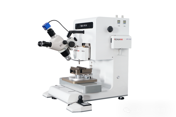
The Alpha W260 push-pull testing machine is a high-precision device designed for microelectronic packaging reliability testing, particularly suitable for the testing needs of semiconductor chip bonding strength:
1. Device Features
High precision: The full range uses a self-developed high-precision data acquisition system to ensure the accuracy of test data.
Functionality: Supports various testing modes, such as chip push testing, gold ball push testing, gold wire tensile testing, and shear force testing.
Ease of operation: Equipped with dedicated software, simple to operate, supports multiple data output formats, and can perfectly match the factory’s SPC network system.
2. Multifunctional Testing Capability
Supports tensile/shear/push testing
Modular design for flexible configuration
3. Intelligent Operation
Automatic data collection
SPC statistical analysis
One-click report generation
4. Safe and Reliable Design
Independent safety limit
Automatic module recognition
Collision prevention protection
5. Fixture System
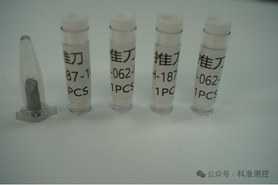
Various specifications of shear tools (suitable for different sizes of solder balls)
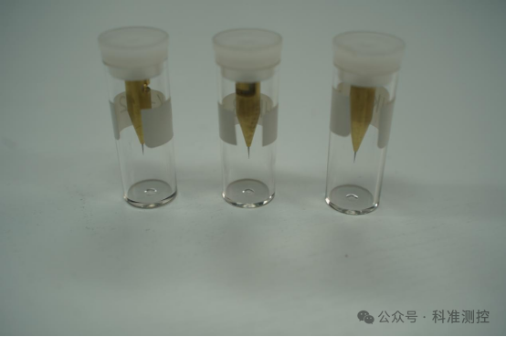
Hook-type tensile fixture
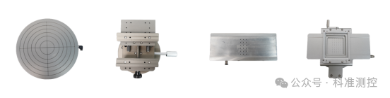
Customized fixture solutions
4. Testing Process
1. Gold wire tensile testing process
Fix the sample on the testing platform
Locate the highest point of the wire arc under a microscope
Slowly raise the hook needle to contact the gold wire
Vertically stretch at a constant speed (0.3mm/s)
Record the maximum tensile force and fracture position
Analyze the failure mode
2. Gold ball push testing process
Horizontally fix the sample
Determine the solder ball height and set the push knife position
Push knife approaches the solder ball horizontally
Apply push force at a speed of 100μm/s
Record the peak push force
Microscope inspection of failure morphology
3. Chip push testing process
Select the long edge of the chip as the testing edge
Align the push knife vertically with the chip edge
Slowly contact to the preset depth
Apply push force until the chip detaches
Record the maximum push force value
Check the residue situation of the chip and substrate
5. Precautions
1. Control of testing environment
Avoid vibration interference
Maintain stable temperature
Implement anti-static measures
2. Instrument calibration
Zero calibration before daily use
Force sensor calibration weekly
Comprehensive system verification monthly
3. Data validity
Test at least 5 points for each sample
Re-test to confirm abnormal values
Retain complete failure photographs
4. Safety regulations
Wear anti-static wrist straps
Avoid collisions during microscope operations
Sharp tools should be stored by designated personnel
The above is the content introduced by the editor regarding the standards and methods for semiconductor chip bonding strength testing. We hope it can be helpful to everyone. If you are also interested in videos and illustrations on how to use push-pull testing machines, usage steps and precautions, operation manuals, principles, calibration and usage method videos, push-pull testing instrument operation specifications, usage methods and testing videos, soldering strength testing instrument usage methods, and bonding tensile testing instruments, feel free to follow us, and you can also send us private messages and comments. The editor of Kezhun Measurement and Control will continue to share potential issues and solutions encountered in the application of push-pull testing machines in fields such as lithium battery resistance, wafers, silicon chips, IC semiconductors, BGA component solder joints, ALMP packaging, microelectronic packaging, LED packaging, and TO packaging.
Previous Reviews
01
|How to test the impact resistance of composite materials? A practical demonstration of the drop hammer testing machine is here
02
|Integrated tensile and torsion testing machine, multi-purpose, testing efficiency doubled!
03
|Why use extensometers in tensile tests? Understand the sources of error and precise measurement methods in one article