Recently, while using the IO ports of STM32 for simulated SPI communication, I encountered a strange phenomenon:
-
Normal Condition: 3.3V push-pull output, waveform is perfect
-
Abnormal Condition: 3.3V to 1.8V, push-pull output with a 4.7K pull-up, SPI timing waveform distortion, data writing is abnormal
Only after increasing the delay can the waveform return to normal! Moreover, the measured voltage is 2V instead of 1.8V. What principle is hidden behind this?The Origin of the Mysterious Voltage: Why is it 2V instead of 1.8V?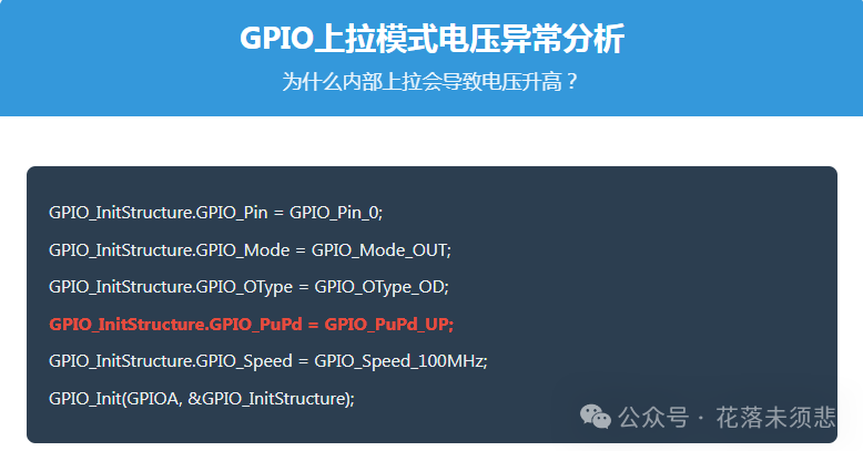 Root Cause of the Problem: The voltage divider effect of internal pull-up and external pull-up resistorsWhen the internal pull-up is enabled, the internal pull-up resistor of the MCU (usually 30-50kΩ) is connected to the 3.3V power supply. Even when set to open-drain output mode, the internal pull-up resistor still operates, forming a resistor divider network with the external 1.8V pull-up, causing the actual measured voltage to rise to about 2.0V.
Solution
When using an external pull-up resistor, the GPIO should be set to<span><span>GPIO_PuPd_NOPULL</span></span> mode to avoid the internal pull-up affecting the voltage level. If reliable level conversion is required, it is best to use a dedicated level conversion chip.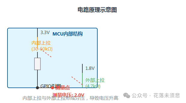 Waveform Distortion Mystery: Why is the OD mode slow to rise?
Root Cause: The contradiction between pull-up resistor value and rise time
The external 4.7K pull-up resistor is relatively large, leading to a longer rise time, which cannot meet the timing requirements of SPI communication. SPI communication has strict timing requirements, and a slow rising edge can cause data instability at the sampling time point.
Comparison of Solutions:
| Solution | Applicable Scenario | Cost | Performance |
|---|---|---|---|
| Open-Drain Output | Medium to Low-Speed Communication | Low | Good |
| Delay Compensation | Temporary Debugging | None | Poor |
| Reduce Pull-Up Resistor | Low Power Requirement Not High | Low | Average |
| Level Conversion Chip | High-Speed Communication | Medium to High | Excellent |
// Increase delay compensation rise timevoid SPI_Delay(void){ for(int i = 0; i < 5; i++); // Adjust delay value}🎯 Key Takeaways
-
Push-pull output + external pull-up = voltage conflict ⚠️
-
Open-drain output is the correct way for level conversion ✅
-
Pull-up resistor value affects rise time 📈
-
In high-speed scenarios, it is recommended to use dedicated level conversion chips 🚀
Remember: When level conversion is needed, always disable the internal pull-up resistor and choose the appropriate pull-up resistor or level conversion chip based on speed requirements!
Be sure to bookmark this article, so you won’t be confused when encountering level conversion issues next time!