As shown in the figure below, the FLUKE5700 uses a patented26bit DAC, which serves as a programmable voltage divider. This DAC is of the pulse width modulation (PWM) type, with linearity better than 1 ppm (parts per million) across the range from one-tenth scale to full scale.
The DAC output voltage is represented in software by what is called the first channel count and the second channel count. Each channel is a 16-bit adjustable duty cycle PWM waveform, with a reference clock of 8 MHz, meaning the minimum pulse width is 62.5 ns. Two PWM signals control MOSFETs to load the reference voltage into a resistor network (HR5), achieving the voltage division ratio.
For example, if the duty cycle of the first channel is10% and the second channel is50%, the overall average voltage is:
(0.1 x 13V) + (0.5 x 0.78 mV) = 1.300390V
The duty cycle resolution is0.0024%, which gives the first channel a resolution of0.309 mV and the second channel a resolution of18.5 nV.
The DAC circuit includes duty cycle control circuits, DAC filtering circuits, linear correction circuits, negative bias circuits, and current sensing elimination circuits.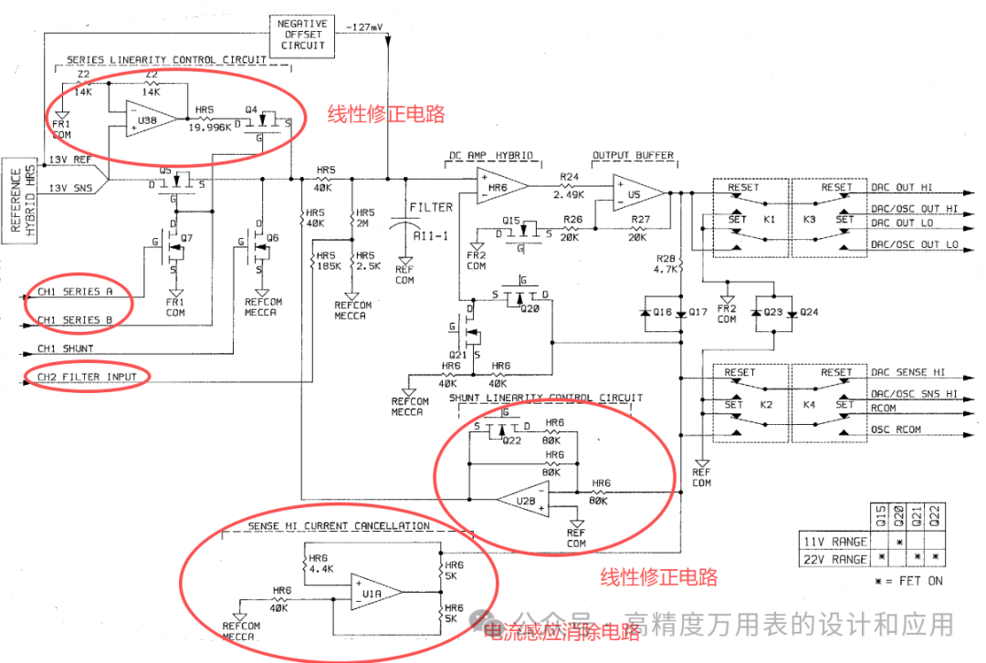
The linear control circuit
includes series linear control circuits and parallel linear control circuits, as shown in the schematic. These linear control circuits eliminate the filtering current in the series switch (Q5) and parallel switch (Q6). This is necessary because Q5 and Q6 have finite resistances (3 to 5 ohms), and slight mismatches in resistance can lead to linear errors.
The series linear control circuit uses operational amplifier U38, a resistor network Z2, and a 19.996 kΩ resistor on the HR5 component. This circuit eliminates the filtering current in the series switch Q5.
When the series switch (FET Q5) is turned on, it connects the 13V reference voltage to the first channel input of the filter, while also turning on FET Q4. This allows U38 to power the filter through the 19.996 kΩ resistor of HR5 and Q4, making the resistance between TP2 and TP5 appear close to 0 ohms. The parallel linear control circuit uses operational amplifier U2B, FET Q22, three 80 kΩ resistors on the HR6 component, and a resistor on the HR5 component. Operational amplifier U2B is configured as an inverting amplifier with a gain of 1 in the 11V range and 0.5 in the 22V range. This gain is determined by FET Q22 and the three 80 kΩ resistors on the HR6 component.
When the parallel switch (FET Q6) is turned on, connecting the filter input to REFCOM, the current in the filter flows through two 40 kΩ resistors on the HR6 component (from pin 7 to pin 8) to the output of U2B. This offsets the current flowing through Q6, making it appear as 0 ohms.
The negative bias circuit
This circuit generates a constant bias voltage of approximately -127 mV at the filter input. Therefore, for the case where the DAC output voltage is 0V, the first channel count must be approximately 400 to offset this negative voltage. This ensures a minimum duty cycle pulse width of about 50 microseconds.
This minimum duty cycle is essential to overcome the bias of the output stage and to allow stabilization after switching the reference voltage to the filter input. Operational amplifier U2A and two 20 kΩ resistors in HR6 form an amplifier with a gain of -1. The input of this amplifier is the 13V reference voltage, and its output generates -13V. The resistors in HR5 divide this -13V to produce -127 mV at the filter input.
The current sensing elimination circuit
This circuit uses operational amplifier U1A and four resistors on the HR6 module. This circuit provides equal but opposite polarity sensing current to the feedback resistors in the 22V range. This eliminates the current in the sensing leads when external sensing occurs.
The DAC filtering circuit
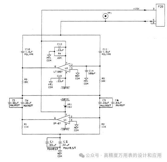
Located on the DAC filtering SIP (A11A1) component. The main pole of the filter is close to 10 Hz. This provides 120 dB attenuation at 190 Hz.
The 30FR1 power supply and the 15V zener diode VR1 create a 15V power supply (15V) for the operational amplifiers in the filtering circuit. The 15V is also connected to the main DAC board and serves as a pull-up resistor for the RANGE SELECT control line along with R111.