Let’s take another look at the DAC output module of the FLUKE5700. All images in this article are sourced from the internet.
The DAC (Digital-to-Analog Converter) is a fundamental component of the calibrator. Other components utilize its precise DC voltage to generate AC and DC voltages and currents.
The DAC consists of five components:
• DAC Main Board (A11)
• DAC Filter SIP (A11A1)
• DAC Buffered Reference SIP (A11A2)
• Reference Hybrid Integrated Block (HR5)
• DC Amplifier Hybrid Integrated Block (HR6)
The DAC components have two main functions:
• Provide high repeatability and stable DC voltage
• Support the calibration of the calibrator’s ADC circuit for completing the calibration.
It consists of an Analog-to-Digital Converter (ADC) and ADC amplifiers. These components work together, requiring only one external voltage source and two external resistance standards to fully characterize the calibrator.
The A11 module is shown in the figure below:
 After removing the shield, we can see its true form:
The dark covers around the HR5 and HR6 hybrid integrated components are not metal, but metallized plastic. The main purpose of these covers is to prevent stray airflow around the reference circuit and DAC pulse amplifiers. This is crucial because parasitic thermoelectric EMF is generated whenever there is a thermal gradient within the circuit board. Additionally, since the hybrid integrated components are actively heated, the covers help maintain thermal stability in the internal constant temperature zone. Don’t forget that the Fluke 5700A consumes a significant amount of power during operation and is equipped with two large fans to provide airflow for the power amplifiers and high-power components and circuit boards.
 The analog acquisition section andPWM generator/ digital controller are enclosed in metal shields on top. This serves a dual purpose, both to contain and localize the generatedRFI/EMI and to provide additional external field shielding. These shields are grounded to the module’s power ground plane.Removing the shield: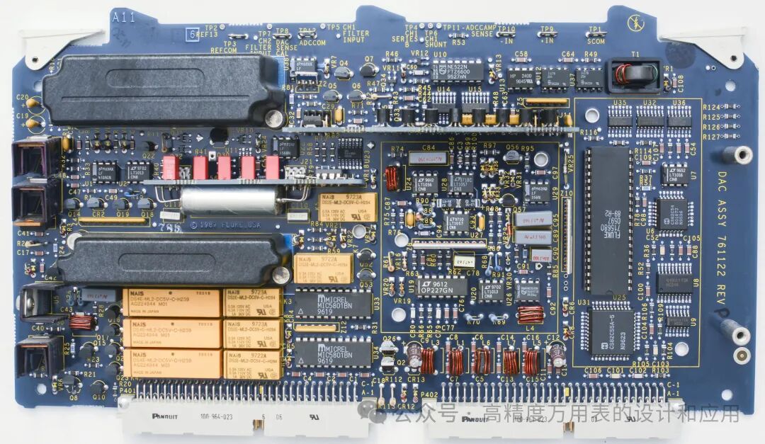
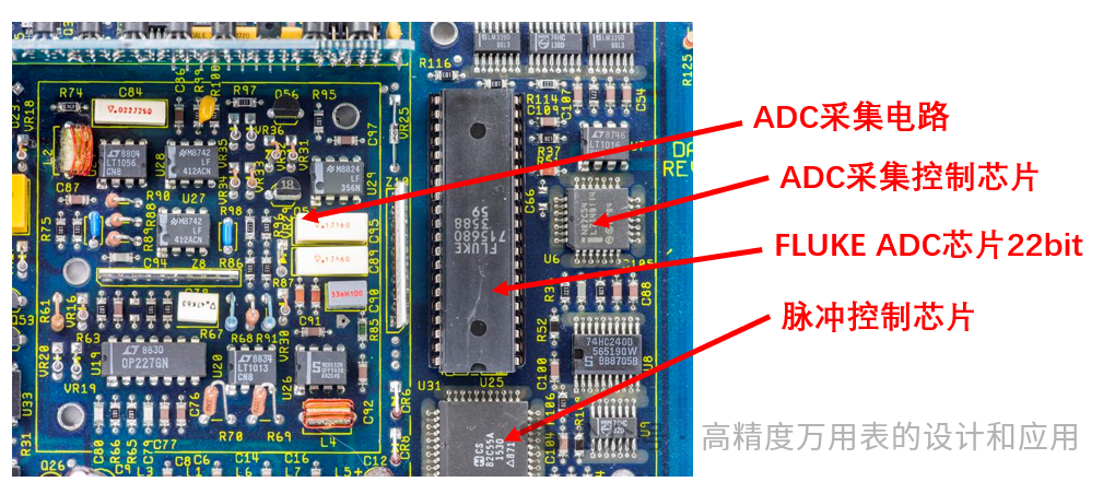
The thermal control HR5 hybrid network with DAC output buffering + thermal control HR6 hybrid network, equipped with reference amplifiers, generates stable 6.xV and 13.xV reference voltages. After removing the covers from HR5 and HR6:
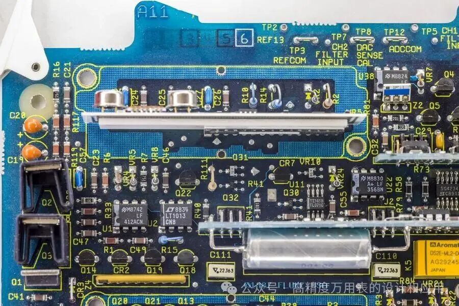
The main DC reference hybrid integrated circuit is constructed from a ceramic substrate sandwich. The main thin substrate contains two reference amplifiers, a hybrid resistor network, several operational amplifiers, temperature resistors, and circuit traces. The back of HR5 has a large area 27-ohm resistor acting as a heater. A spacer is then glued on, serving as a heat sink, coupled with a sealed hybrid resistor that has a transparent quartz window for laser trimming.
The 13V reference voltage consists of two cascaded 6.5V temperature-compensated transistor/Zener diode pairs, known as reference amplifiers (U6 and U7). The excellent temperature characteristics of the reference amplifiers are achieved by applying appropriate bias to the collector current of their transistors, offsetting the temperature coefficient (TC) of the Zener diode with that of the base-emitter junction. Since the base-emitter junction and the Zener diode are in series, the result is a near-zero temperature coefficient.
The design of the reference amplifiers ensures that the influence of thin-film resistor and operational amplifier errors is second-order. Therefore, the accuracy is almost entirely determined by the reference amplifiers.
Aside from the reference amplifiers (Ref-Amps), all components are surface-mounted, with the reference amplifiers being Motorola SZA263. Using two reference amplifiers provides a higher 13 VDC (6.5 + 6.5) reference level, further reducing noise and improving DAC stability. The excellent temperature coefficient of the reference amplifiers is achieved through stable transistor collector bias current provided by stable thin-film resistors between the reference amplifiers. This design minimizes the impact of circuit component errors on the output voltage, making its output stability almost entirely dependent on the performance of the Motorola SZA263.

To prevent output drift with environmental temperature, the entire component is heated to a constant 62°C via an external circuit module on the main A11 PCB. The temperature feedback element is a thermistor RT1, located next to the reference amplifier package. Since ceramics are good thermal conductors, temperature changes in the hybrid integrated module drive a correction signal for Q2, adjusting power to the 27-ohm thin-film resistor to return the temperature to the set point. There is also thermal runaway protection, implemented by a second thermistor RT2, which activates Q9 to bypass the base current of Q1 to prevent overheating. This protection activates when the board temperature reaches 67°C, but should never be used under normal conditions.
Interestingly, according to information provided by zlymex, the improved Fluke 5720A has also seen changes in its HR5 DC reference hybrid integrated module.
A pair of Motorola SZA263 chips has been replaced by Linear LTFLU-1ACH, and the LF351 op-amp has been replaced by Linear LT1006 and TL071C. The hybrid laser-trimmed resistor network is smaller and has a different configuration.

To be continued…