Definition of PCB Layers:
Solder mask layer: solder mask, refers to the part of the board where green oil is applied; since it is a negative output, the part with solder mask actually does not have green oil but is plated with tin, appearing silver-white!
Paste mask layer: paste mask, is used during machine placement, corresponding to the pads of all surface mount components, its size is the same as the toplayer/bottomlayer, and it is used for stencil solder paste application.
Key points: Both layers are for soldering, not one for soldering and one for green oil; so is there a layer that indicates the area for applying green oil? As of now, I have not encountered such a layer! In the PCB we design, the pads by default have a solder layer, so the manufactured PCB pads are plated with silver solder, which is not surprising that they do not have green oil; however, the routing part of the PCB we design only has the toplayer or bottomlayer, without a solder layer, but the manufactured PCB routing part has a layer of green oil applied.
We can understand it this way: 1. The solder mask layer means opening windows on the entire solder mask green oil, to allow for soldering! 2. By default, areas without a solder mask layer must have green oil applied! 3. The paste mask layer is used for surface mount packaging! SMT packaging uses: toplayer layer, topsolder layer, toppaste layer, and the toplayer and toppaste are the same size, while the topsolder is larger by one circle. DIP packaging only uses: topsolder and multilayer (after some decomposition, I found that the multilayer actually overlaps the sizes of toplayer, bottomlayer, topsolder, and bottomsolder), and the topsolder/bottomlayer is larger by one circle.
Question: “The statement that the copper layer corresponding to the solder layer has copper will be plated with tin or gold” is correct? This statement was made by someone working in a PCB factory, meaning that in order for the part drawn on the solder layer to be plated with tin, the corresponding solder layer must have copper (i.e., the area corresponding to the solder layer must have parts of the toplayer or bottomlayer)! Now, I conclude: “The statement that the copper layer corresponding to the solder layer has copper will be plated with tin or gold” is correct! The solder layer indicates areas that are not covered by green oil!
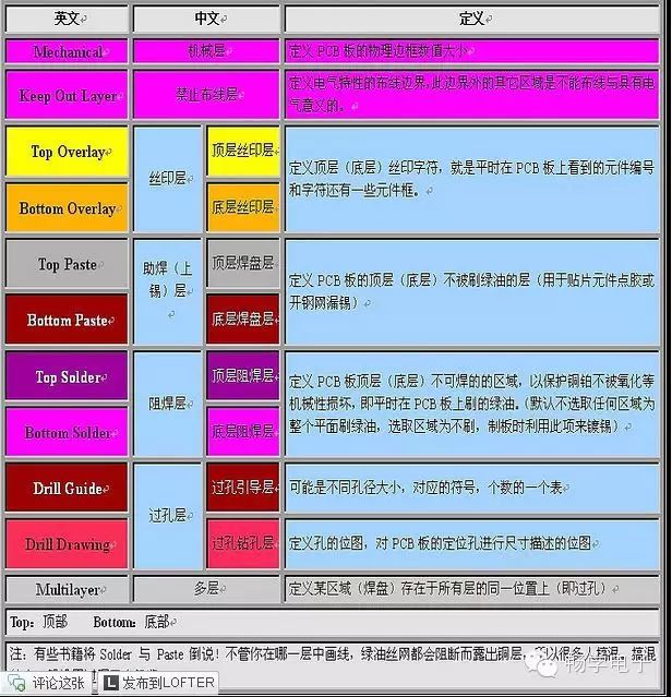
Mechanical layer, mechanical layer
Keepout layer, prohibited wiring layer
Top overlay, top silkscreen layer
Bottom overlay, bottom silkscreen layer
Top paste, top pad layer
Bottom paste, bottom pad layer
Top solder, top solder mask layer
Bottom solder, bottom solder mask layer
Drill guide, drill guide layer
Drill drawing, drill hole layer
Multilayer, multilayer
The mechanical layer defines the appearance of the entire PCB board; when we refer to the mechanical layer, we are actually referring to the overall shape structure of the PCB board. The keepout layer defines the boundaries for placing electrical characteristic copper, meaning that after defining the keepout layer, the lines with electrical characteristics we place in the future cannot exceed the boundaries of the keepout layer. The top overlay and bottom overlay define the silkscreen characters on the top and bottom layers, which are generally the component numbers and some characters we see on the PCB board. The top paste and bottom paste refer to the layers of pads that are visible, (for example, if we draw a wire in the top layer, what we see on the PCB is just a wire, covered by green oil, but at the position of this wire, we draw a square or a dot on the toppaste layer, the square and dot made on the board will not have green oil, but will be copper pads. The top solder and bottom solder layers are just the opposite of the previous two layers; we can say that these two layers are the layers that need to cover green oil. The multilayer layer is actually similar to the mechanical layer, as the name implies, this layer refers to all layers of the PCB.
The distinction between solder mask layer and paste mask layer
The solder mask layer: solder mask, refers to the part of the board where green oil is applied; since it is a negative output, the part with solder mask actually does not have green oil but is plated with tin, appearing silver-white!
The paste mask layer: paste mask, is used during machine placement, corresponding to the pads of all surface mount components, its size is the same as the toplayer/bottomlayer, and it is used for stencil solder paste application.
Key points: Both layers are for soldering, not one for soldering and one for green oil; so is there a layer that indicates the area for applying green oil? As of now, I have not encountered such a layer! In the PCB we design, the pads by default have a solder layer, so the manufactured PCB pads are plated with silver solder, which is not surprising that they do not have green oil; however, the routing part of the PCB we design only has the toplayer or bottomlayer, without a solder layer, but the manufactured PCB routing part has a layer of green oil applied.
We can understand it this way: 1. The solder mask layer means opening windows on the entire solder mask green oil, to allow for soldering! 2. By default, areas without a solder mask layer must have green oil applied! 3. The paste mask layer is used for surface mount packaging! SMT packaging uses: toplayer layer, top solder layer, top paste layer, and the toplayer and top paste are the same size, while the top solder is larger by one circle. DIP packaging only uses: top solder and multilayer (after some decomposition, I found that the multilayer actually overlaps the sizes of toplayer, bottomlayer, topsolder, and bottomsolder), and the topsolder/bottomlayer is larger by one circle.