When designing multilayer PCBs, it is essential to configure the layering. The more layers a board has, the more layering schemes are available. Many people are not well-versed in multilayer PCB stacking, and a good layering scheme can reduce interference generated by the board. Our stacking structure is a crucial factor affecting the EMC performance of the PCB. Below, we will introduce the layering schemes for four-layer and six-layer boards, allowing us to select the optimal stacking structure.
For four-layer boards, there are three common stacking structures:
First:
Second:
Third:
First, let’s analyze the first and second stacking schemes. The difference between these two stacking schemes is that the second and third layers are reversed. Both are commonly used stacking schemes for four-layer boards. Both schemes are feasible, but the selection should be based on the actual conditions of our board. Typically, when designing a four-layer board, we primarily consider whether the components are placed on the top or bottom layer. Our GND layer should be placed close to the component layer to provide a complete ground plane, which can also shield against interference. Additionally, our routing should ideally be done on the bottom layer to ensure signal stability and avoid cross-segmentation. This is the difference between these two stacking schemes. Next, let’s look at the third stacking scheme. This scheme distributes the layers and power across the first and fourth layers. In a two-layer board, we need to handle our signal lines, ground, and power on the top and bottom layers. However, since this is a four-layer board, using this stacking scheme negates the advantages of a four-layer board, and the signal quality is also poor. The second and third layers are routing layers. First, we need to know that our components should be placed on the top and bottom layers. If we allocate the top and bottom layers for ground and power, we cannot ensure the integrity of the ground plane, and the same goes for power. This means that the routing on the second and third layers may not have a complete reference plane, and the interference shielding of this stacking scheme is also poor. Typically, after completing the board design, we need to cover the top and bottom layers with a full ground copper layer. Therefore, having the first layer as the ground layer in this stacking scheme is somewhat redundant, making this stacking scheme unsuitable for standard four-layer PCB designs. The above describes the common stacking schemes for four-layer boards. We can select between the first and second stacking schemes based on the actual conditions of the board. Next, we will introduce the common stacking schemes for six-layer boards.
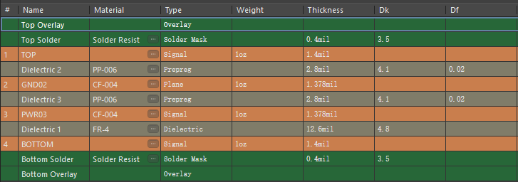
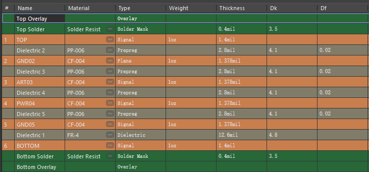
First:
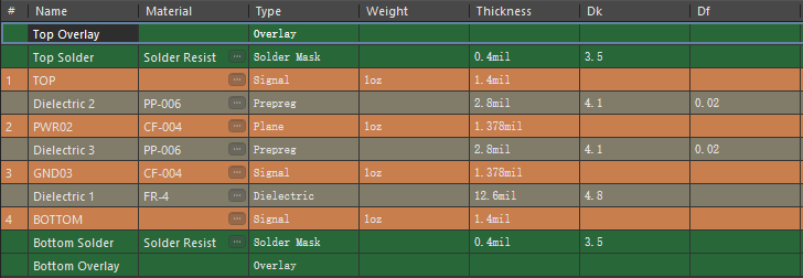
Second:
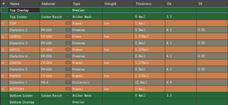
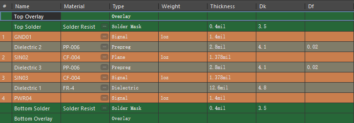
Third:
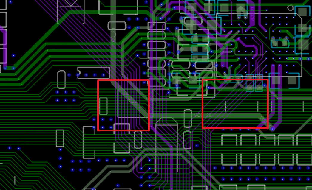
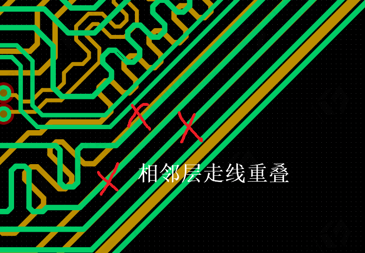
The first stacking scheme has two routing layers, which can reduce our routing difficulty. However, the third and fourth layers are adjacent routing layers, which can easily cause crosstalk. Therefore, when adopting this stacking scheme, we must pay special attention to using perpendicular routing for adjacent layers to avoid parallel routing (as shown in the figure below).
The second stacking scheme has the third layer as the signal layer, with adjacent layers being GND, allowing for effective isolation from other layers and reducing the likelihood of crosstalk. However, having only one internal routing layer may increase the difficulty of routing, so careful planning of routing channels and paths is necessary to ensure all signal lines can be handled. Additionally, since the first three layers have only one internal power layer and the last three layers have two internal power layers, this asymmetry in internal power layers can lead to warping risks.The third stacking scheme is similar to the second, with only the fourth and fifth layers swapped. This stacking scheme can also provide effective isolation for our signals, but it also has the issue of internal power layers not being aligned, which can lead to warping. This stacking scheme has two adjacent ground layers, which can improve signal quality. In design, many clients may require two reference planes for controlled impedance lines, and more stringent designs may require two ground planes, necessitating the integrity of the reference planes. Generally, ground planes are relatively complete, while power planes often need to handle different power signals. If two adjacent planes are required for reference, there is a risk of cross-segmentation.From the above discussion, we find that each stacking scheme has its advantages and disadvantages. We need to select the appropriate stacking scheme based on the actual conditions of the board. In practical design, we find that the first stacking scheme is used particularly frequently because ordinary companies also need to consider costs; they prefer not to add layers due to the high costs associated with additional layers, especially evident in mass production. When the number of lines is not particularly high, we prioritize selecting the second and third stacking schemes, which also ensure signal quality. For military companies, cost is secondary; they first consider the signal quality of the board and then consider costs while ensuring signal quality. The above describes the stacking schemes for four-layer and six-layer boards. Although we only introduced the stacking for four-layer and six-layer boards, we can analyze higher-layer PCBs similarly, determining the number of layers based on board density and structure, and then selecting an appropriate stacking scheme based on the number of layers.

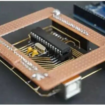
Using iron wire to make a “circuit board”, you have to admire this operation!

If you understand these issues, you are a qualified hardware engineer.

Scan to add customer service WeChat, note “Join Group” to pull you into the official Fanyi Education technical WeChat group to discuss technical issues and insights with many electronic technology experts~
Share 💬 Like 👍 Look ❤️ Support with a “triple click”!
Click “Read the original” to see more exciting articles.