Hello everyone, I am Goat.
Continuing with some other signal quality issues related to I2C. If you encounter these problems, how can you resolve them?
-
Back Reflection
Back reflection poses significant risks to clock-type signals, and since the I2C CLK signal is a clock-type signal, the presence of back reflection can lead to sampling errors. For instance, it may sample extra data, directly affecting the monotonicity of the rising and falling edges of the clock signal.
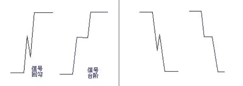
In the case of the system power supply, back reflection on the power-up edge may cause the system to crash. The specific situation needs to be evaluated in conjunction with the reset signal to determine if it is acceptable.
If back reflection occurs in the data signal, since data signals are generally sampled in the middle of the data, the impact of back reflection is relatively small. However, there are certain situations that require special attention, such as when the rise time is very fast or when the setup and hold times are very short, on the order of a few ns, where the impact of back reflection on the overall data must be considered.

So, what causes back reflection in I2C signals?
The reason may also be due to impedance mismatch causing reflections, which then superimpose on the waveform edges, leading to the appearance of back reflection or steps. It may also be due to improper termination or issues in the PCB design, such as stub problems, etc.
How to resolve it?
To address back reflection, appropriate matching can be added. For single-ended signals, a 33Ω resistor is generally used for matching.
-
Slow Edges
The issue of slow edges mainly leads to sampling errors. For example, when the rising and falling edges of the data signal occur slowly, it can cause data sampling errors. Therefore, when capturing I2C signals, it is necessary to check whether the rise and fall times of the signal meet the specifications.
So, what causes slow edges in I2C signals?
The main reasons may be insufficient drive capability or excessive load, such as long traces or significant parasitic capacitance.
How to resolve it?
The main approach is to increase the drive capability. Specifically, this can be achieved by reducing resistance to increase current, thereby enhancing drive capability, or by reducing the load (in cases of excessive load).
(Other notes:
STUB issues: The stub problem refers to a protruding structure on the PCB. Some engineers may inadvertently or inevitably design extra wiring ends, also known as stubs or remnants, during the PCB design process. These extra wire ends may produce antenna radiation effects.

As a result, signal reflections may occur, leading to signal integrity issues. Additionally, for some high-speed signals, the stubs created by vias must also be considered.
Previous Exciting Content:
Additional Insights on I2C Signal Quality Issues (Part 1)
The Rich Guy of Capacitors – Tantalum Capacitors
Understanding QSPI Signal Protocol in Simple Terms (Part 2)
Can Hardware Engineers Find Jobs Right at Their Doorstep?
Click here👇 to follow for more updates~
One-click triple connection: “Share”, “Like”, and “View”
Updates 2-4 times a week~