▲ Click the blue text above to follow us and not miss any valuable articles!
This application note provides guidance and recommendations on the design and layout of radio frequency (RF) printed circuit boards (PCBs), including discussions on mixed-signal applications, such as digital, analog, and RF components on the same PCB. The content is organized by topic and provides “best practice” guidelines that should be applied in conjunction with all other design and manufacturing guidelines that may apply to specific components, PCB manufacturers, and materials.
PCB Layout Principles for RF Boards
Layout Determination: Before layout, a detailed understanding of the single board’s functions, operating frequency bands, current and voltage, main RF component types, EMC, and relevant RF metrics is essential. Additionally, the stack-up structure, impedance control, dimensions of the outline structure, shielding cavity, and cover size and position, as well as special processing instructions for components (such as cutouts and direct heat dissipation from the casing) should be clarified. Furthermore, the main RF component’s power, heat dissipation, gain, isolation, sensitivity, and the connections of filtering, biasing, and matching circuits should be defined. For power amplifier circuits, the recommended matching routing requirements from the component datasheet or impedance matching circuit guidance obtained from RF field analysis software simulations should be followed.Physical Partitioning: The key is to arrange the main components based on the primary signal flow direction of the single board. First, fix the components on the RF path according to the RF port position and adjust their orientation to minimize the length of the RF path. In addition to considering general layout rules, it is also necessary to reduce mutual interference between different parts and enhance anti-interference capability, ensuring sufficient isolation between multiple circuits. For circuits with insufficient isolation or those that are sensitive or have strong radiation sources, consider using metal shielding to confine RF energy within the RF area.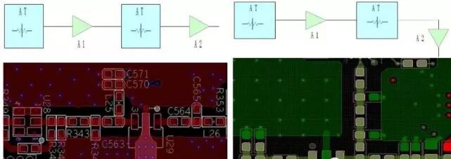 Electrical Partitioning: The layout is generally divided into three parts: power, digital, and analog, which should be spatially separated, and routing should not cross regions. Strong and weak signals should be separated as much as possible, and circuits that perform the same function should be arranged within a certain range to minimize the signal loop area.
RF Transmission Lines
Many Maxim RF components require controlled impedance transmission lines to transmit RF power to the IC pins on the PCB (or from them). These transmission lines can be implemented on the outer layers (top or bottom) or buried in the inner layers. Guidelines for these transmission lines include discussions on microstrip lines, strip lines, coplanar waveguides (ground), and characteristic impedance. It also covers transmission line bend compensation and layer transitions.
Microstrip Lines
This type of transmission line consists of fixed-width metal traces (conductors) and a ground area directly below (in the adjacent layer). For example, traces on layer 1 (top metal) require a solid ground area on layer 2 (Figure 1). The width of the traces, the thickness of the dielectric layer, and the type of dielectric determine the characteristic impedance (typically 50Ω or 75Ω).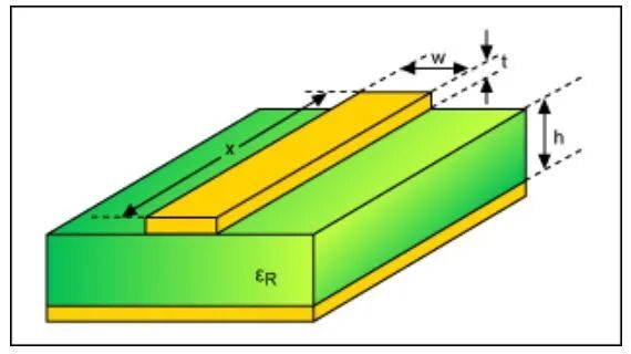
Strip Lines
This type includes fixed-width traces in the inner layer, with ground areas above and below. The conductors can be centered in the ground area (Figure 2) or offset (Figure 3). This method is suitable for RF traces in the inner layer.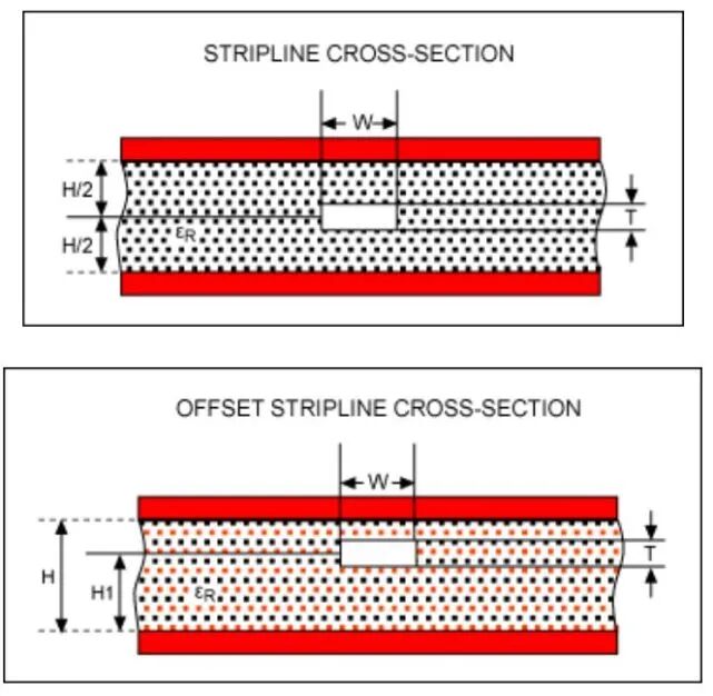
Coplanar Waveguides (Ground)
Coplanar waveguides provide better isolation between adjacent RF lines and other signal lines (end view). This dielectric includes a center conductor and ground areas on both sides and below (Figure 4). It is recommended to install via “fences” on both sides of the coplanar waveguide, as shown in Figure 5. The top view provides an example of installing a row of ground vias in the top metal area on each side of the center conductor. The return current induced on the top layer is shorted to the ground layer below.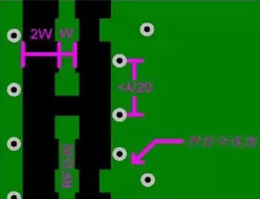
Characteristic Impedance
There are various calculation tools (recommended to use the PCB characteristic impedance calculator Polar SI9000) available to correctly set the signal conductor trace width to achieve the target impedance. However, care should be taken when inputting the dielectric constant of the board layer. The typical dielectric constant of the outer substrate layer of a PCB contains less fiberglass than the inner layers, resulting in a lower dielectric constant. For example, the dielectric constant of FR4 material is generally εR = 4.2, while the outer substrate (prepreg) layer is generally εR = 3.8. The example below is for reference, where the metal thickness is 1oz copper (1.4 mils, 0.036mm).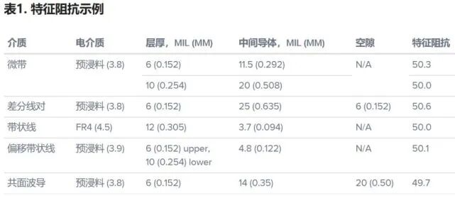
Transmission Line Bend Compensation
When routing constraints require bending the transmission line (changing direction), the bend radius used should be at least three times the width of the center conductor. That is:Bend radius ≥ 3 × (line width)This minimizes the change in characteristic impedance at the bend point.If gradual bending is not possible, the transmission line can be bent at right angles (non-curved), as shown in Figure 6. However, compensation must be applied to reduce the impedance discontinuity caused by the local effective line width increase at the bend point. The standard compensation method is to chamfer the corners, as shown in the figure below. The optimal microstrip right-angle chamfer is given by the Douville and James formula:Where M is the ratio of the chamfered to non-chamfered bend angle (%). This formula is independent of the dielectric constant, with the constraint being w/h ≥ 0.25.Other transmission lines can use similar methods. If there is any uncertainty about the correct compensation method, and the design requires high-performance transmission lines, electromagnetic simulators should be used to model the bends.
Layer Transition of Transmission Lines
If layout constraints require transitioning the transmission line to a different PCB layer, it is recommended to use at least two vias for each transmission line to minimize via inductance loading. A pair of vias effectively reduces the transmission inductance by 50%, and the maximum diameter of the vias should be comparable to the width of the transmission line. For example, for a 15-mil microstrip line, the via diameter (plated through-hole diameter) should be between 15 mil and 18 mil. If space does not allow for large vias, three smaller transition vias should be used.
Signal Line Isolation
Care must be taken to prevent unintended coupling between signal lines. Below are examples of potential coupling and preventive measures:RF Transmission Lines: The distance between transmission lines should be as large as possible and should not be close to each other over long distances. The smaller the spacing and the longer the parallel routing distance, the greater the coupling between parallel microstrip lines. Traces on different layers should have ground areas to keep them separated. High-power transmission lines should be kept as far away from other transmission lines as possible. Grounded coplanar waveguides provide excellent inter-line isolation. Isolation between RF lines on small PCBs is unrealistic to exceed about -45dB.High-Speed Digital Signal Lines: These signal lines should be laid out independently on different PCB layers from RF signal lines to prevent coupling. Digital noise (from clocks, PLLs, etc.) can couple into RF signal lines, modulating the RF carrier. In some cases, digital noise can be upconverted/downconverted.VCC/Power Lines: These lines should be laid out on dedicated layers. Appropriate decoupling/bypass capacitors should be installed at the main VCC distribution nodes and VCC branches. Bypass capacitors must be selected based on the overall frequency response of the RF IC and the expected frequency distribution of digital noise caused by clocks and PLLs. These traces should also be isolated from RF lines, which will emit larger RF power.
Ground Areas
If layer 1 is used for RF components and transmission lines, it is recommended to use solid (continuous) ground areas on layer 2. For strip lines and offset strip lines, ground areas are required above and below the center conductor. These areas should not be shared or allocated to signal or power networks but must be entirely allocated to ground. Sometimes, due to design constraints, a local ground area on a certain layer must be located directly beneath all RF components and transmission lines. Ground areas should not be interrupted beneath transmission lines.A large number of ground vias should be arranged between different layers of the RF section of the PCB. This helps prevent parasitic ground inductance from increasing due to ground current loops. Vias also help prevent cross-coupling between RF signal lines and other signal lines on the PCB.
Special Considerations for Power and Ground Layers
For PCB layers allocated to system power (DC power) and ground, the loop currents of the components must be considered. The general principle is to avoid routing signal lines on PCB layers between power and ground layers.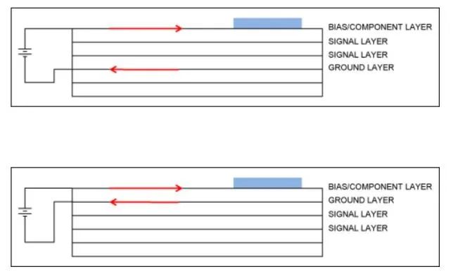
Power (Bias) Traces and Power Decoupling
If components have multiple power connections, a common practice is to use a “star” configuration for power wiring (Figure 9). Install larger decoupling capacitors (tens of µF) at the “root” node of the star configuration, and smaller capacitors on each branch. The values of these small capacitors depend on the operating frequency of the RF IC and its specific functions (i.e., inter-stage and main power decoupling). The diagram below shows an example.Compared to a configuration where all pins connected to the same power network are in series, the star configuration avoids long ground loops. Long ground loops can cause parasitic inductance, leading to unintended feedback loops. A key consideration for power decoupling is that the DC power must be electrically defined as AC ground.
Selection of Decoupling and Bypass Capacitors
Due to the self-resonant frequency (SRF), the effective frequency range of capacitors is limited in practice. SRF can be obtained from manufacturers, but sometimes must be characterized through direct measurement. Above the SRF, capacitors exhibit inductive behavior, thus lacking decoupling or bypass functionality. For wideband decoupling, the standard practice is to use multiple capacitors (of increasing capacitance values) in parallel. Small capacitors generally have a larger SRF (e.g., 0.2pF, 0402 SMT package capacitor SRF = 14GHz), while larger capacitors generally have a smaller SRF (e.g., the same package 2pF capacitor SRF = 4GHz). Table 2 lists typical configurations.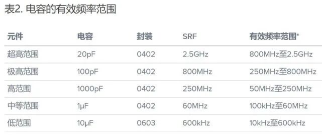 * The low end of the effective frequency range is defined as below 5Ω capacitive reactance.
Bypass Capacitor Layout Considerations
Since power lines must be AC ground, it is crucial to minimize parasitic inductance in the AC ground loop. The layout or orientation of components can introduce parasitic inductance, such as the direction of decoupling capacitors. There are two placement methods for bypass capacitors, as shown in Figures 10 and 11: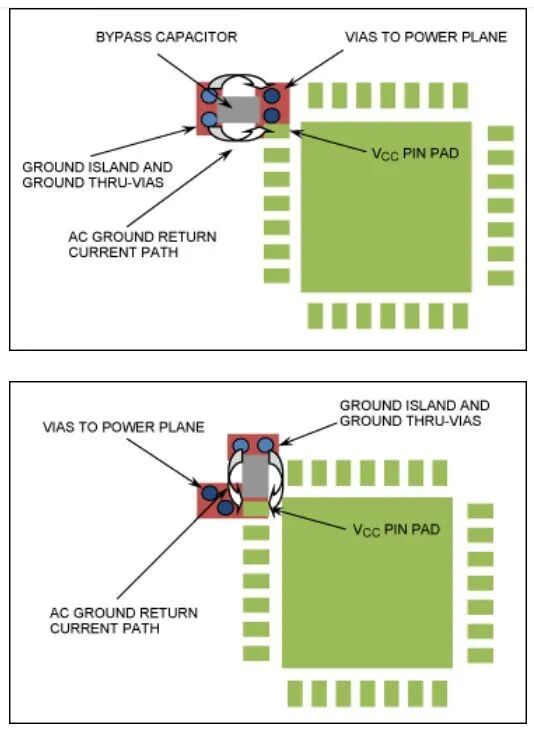 In this configuration, connecting the VCC pad on the top layer to the via of the inner power area (layer) may hinder the AC ground current loop, forcing a longer loop and resulting in higher parasitic inductance. Any AC current flowing into the VCC pin passes through the bypass capacitor to its ground side and then returns to the internal ground layer. In this configuration, the total footprint area of the bypass capacitor and associated vias is minimized.In another configuration, the AC ground loop is not restricted by the power area vias. Generally, this configuration requires slightly larger PCB area.
Grounding of Short-Circuit Connected Components
For components connected to ground via short-circuit connections (e.g., power decoupling capacitors), it is recommended to use at least two ground vias for each component (Figure 12), which can reduce the impact of via parasitic inductance. Groups of short-circuit connected components can use via grounding “islands”.
IC Grounding Areas (“Pads”)
Most ICs require solid ground areas on the component layer (top or bottom of the PCB) directly beneath the component. This ground area will carry DC and RF return currents flowing through the PCB to the allocated ground area. The second function of this component “ground pad” is to provide heat dissipation, so the pad should include the maximum number of vias allowed by the PCB design rules. In the example shown below, a 5 × 5 array of vias is installed in the center ground area directly beneath the RF IC (Figure 13). Where other layout considerations allow, the maximum number of vias should be used. These vias should be ideal through holes (penetrating the entire PCB). These vias must be plated. If possible, thermal conductive glue should be used to fill the vias to enhance heat dissipation (after plating the vias and before the final plating of the PCB).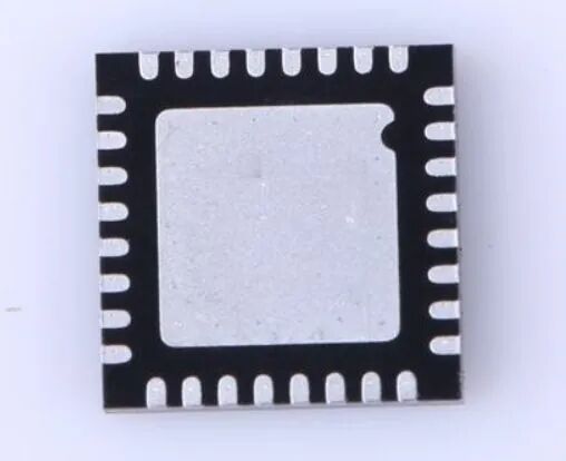
Shielding Covers
PCB shielding involves metallic isolation between two spatial areas to control the induction and radiation of electric fields, magnetic fields, and electromagnetic waves from one area to another. Specifically, it involves surrounding the interference sources of components, circuits, assemblies, cables, or entire systems with PCB shielding to prevent the interference electromagnetic field from spreading outward; and surrounding receiving circuits, devices, or systems with PCB shielding to protect them from external electromagnetic fields.
Several Wiring Layout Guidelines
1. RF link linear layout: When laid out within the same shielding cavity, signals can be arranged in a linear or L-shape from small to large. Shielding isolation should be added between strong and weak signals, and shielding measures should also be taken on branches with larger gain. In the same shielding cavity, avoid Z-shaped, U-shaped, or crossed layouts as much as possible.2. For a PI-type attenuator composed of three resistors, the pads can be placed on the microstrip line and should not bend, as shown in Figure 1. If layout space is tight, the two grounding resistors should be placed on the shortest high-resistance branch possible.3. The layout of the feed inductance for the bias circuit: Do not run parallel to the RF channel; it is best to run perpendicular to the RF line.4. As much as possible, isolate high-power RF amplifiers (HPA) from low-noise amplifiers (LNA), keeping high-power RF transmission circuits away from low-power RF reception circuits.5. The RF output should be as far away from the RF input as possible to prevent output signals from coupling into the input.6. Decoupling capacitors should be placed close to the components that need protection; decoupling capacitors for ESD-sensitive components should be close to the component’s power and ground pins.7. The output of filters should be as close as possible to the voltage-controlled oscillator (VCO) input, distributed according to the minimum process spacing.8. Attenuator networks used to improve the port matching of dielectric filters should be close to the dielectric filter ports; otherwise, severe mismatch at the filter port can lead to strong reflections, which may cause out-of-band self-oscillation when cascaded with amplifiers.9. The width of the shielding cavity wall should be greater than 1MM, and it is recommended that the pads of the components inside the cavity be at least 2mm away from the cavity edge. Other signals should be at least 0.5mm away from the cavity. Additionally, fixed mounting holes should be added at the corners of the cavity, with holes being 2.8-3mm.10. As much as possible, keep digital circuits away from analog circuits, ensuring that RF traces reference a large area ground plane and that RF traces are routed on the surface layer.11. Digital and analog signal lines should not cross regions; if RF traces must pass through signal lines, the preferred option is to route a ground plane connected to the main ground along the RF trace between them; the second option is to ensure that RF lines and signal lines cross at right angles, minimizing capacitive coupling while adding as much ground as possible around each RF trace and connecting it to the main ground. Generally, RF printed traces should not be routed in parallel and should not be excessively long; if parallel routing is necessary, a ground trace should be added between the two lines (ground trace should have vias to ensure good grounding). For RF differential lines, run parallel lines with ground traces on the outside (ground trace should have vias to ensure good grounding), and design the printed trace’s characteristic impedance according to the device’s requirements.12. The basic order of RF printed circuit board wiring: RF line baseband RF interface line (IQ line) clock line power section digital baseband section ground.13. Considering that green oil can affect the performance and signals of microstrip lines, it is recommended that high-frequency single-board microstrip lines not be coated with green oil, while mid-low frequency single-board microstrip lines should be coated with green oil.14. RF traces should generally not have vias; if RF traces must transition layers, the via size should be minimized to reduce path inductance and the opportunity for RF energy to leak into other areas of the stack-up.15. Duplexers, intermediate frequency amplifiers, and mixers often have multiple RF/IF signals interfering with each other; RF and IF traces should cross at right angles as much as possible, with a ground area in between.16. Unless for special purposes, RF signal traces should not extend beyond the necessary length.17. Baseband RF interface lines (IQ lines) should be wider, preferably over 10mil, to avoid phase errors, with lengths as equal as possible and spacing as equal as possible.18. RF control lines should be as short as possible, adjusting the trace length according to the input/output impedance of the transmission control signal device to reduce noise introduction. Traces should be kept away from RF signals, non-metalized holes, and the edges of the “ground”. No ground vias should be placed around the traces to prevent signals from coupling through vias to the RF ground.19. As much as possible, keep digital traces and power traces away from RF circuits; clock circuits and high-frequency circuits are major sources of interference and radiation and should be arranged separately, away from sensitive circuits.20. The main clock trace should be as short as possible, with a recommended width of over 10mil, and ground should be wrapped around both sides to prevent interference from other signal lines. It is recommended to use strip line forms for routing.21. Digital and analog signal lines should not cross regions; if signal traces must pass through RF lines, the preferred option is to layer the routing, placing a ground plane connected to the main ground along the RF trace between them; the second option is to cross RF lines and signal lines at right angles, allowing lower frequency digital signals to pass vertically between large package capacitor pads while adding as much ground as possible around each RF trace and connecting it to the main ground. Additionally, minimizing the parallel length between RF traces can minimize inductive coupling.22. Control lines for voltage-controlled oscillators (VCOs) must be kept away from RF signals, and if necessary, ground shielding can be applied to the VCO control lines.23. On every layer of the PCB, as many grounds as possible should be laid out and connected to the main ground. Traces should be kept close together to increase the number of ground blocks between internal signal layers and power distribution layers.24. Impedance: RF line impedance is 50 ohms, and the trace width should be as wide as possible while meeting impedance requirements. The trace width should be as close as possible to the size of 0603 passive components.25. Corners: If RF signal traces make right angles, the effective line width at the corners will increase, causing impedance discontinuities and reflections. Therefore, corners should be treated, primarily with chamfers and rounded corners.26. Transition Lines: Some RF component packages are small, and SMD pad widths may be as small as 12mils, while RF line widths may reach 50mils; it is recommended to use transition lines and prohibit sudden changes in line width.27. RF signals should generally not have vias; if vias are necessary for layer transitions, RF engineers should calculate the appropriate via size through simulation. Additionally, minimize the impedance discontinuity of vias using common methods such as using blind vias, selecting appropriate routing methods, and optimizing solder pad diameters.28. The maximum spacing for vias under large pads of RF components is approximately λ/10, with a minimum spacing of about λ/60. The blank area in the RF region should be covered with a large area of ground copper, fully connected, with vias punched in the ground copper. Ground vias should be added at positions close to the shielding cavity walls, with at least two rows of vias and a spacing of less than λ/20.29. Microstrip Line Routing: RF signals should be routed on the top layer of the PCB, and the plane layer beneath the RF signal must be fully grounded to form a microstrip line structure.30. The edge of the microstrip line should be at least 3W away from the edge of the underlying ground plane, and there should be no non-grounded vias within the 3W range.31. The distance from the microstrip line to the shielding wall should be maintained at over 2W, at least 20mil.32. Non-coupled microstrip lines within the same layer should be treated with ground copper and have ground vias added to the ground copper, with a spacing of less than λ/20, arranged uniformly and neatly. The edges of the ground copper foil should be smooth and flat, with no sharp burrs. It is recommended that the edges of the ground copper foil be at least 2W or 3H away from the edges of the microstrip line, where H represents the thickness of the microstrip substrate dielectric.33. RF signal traces should not cross gaps in the ground plane of the second layer.34. Strip Line Routing: RF signals should pass through the middle layer of the PCB, typically from the third layer, with the second and fourth layers fully grounded, forming an eccentric strip line structure.35. The edges of the strip line should be at least 3W away from the edges of the upper and lower ground planes, and there should be no non-grounded vias within the 3W range.36. Strip lines within the same layer should be treated with ground copper and have ground vias added to the ground copper, with a spacing of less than λ/20, arranged uniformly and neatly. The edges of the ground copper foil should be smooth and flat, with no sharp burrs. It is recommended that the edges of the ground copper foil be at least 2W or 3H away from the edges of the strip line, where H represents the total thickness of the dielectric layers above and below the strip line.37. If the strip line is to transmit high-power signals, to avoid the 50-ohm line width being too thin, the copper planes of the upper and lower reference planes of the strip line area should be hollowed out, with a hollow width of more than 5 times the total dielectric thickness of the strip line. If the line width still does not meet the requirements, the adjacent second layer reference plane should also be hollowed out.
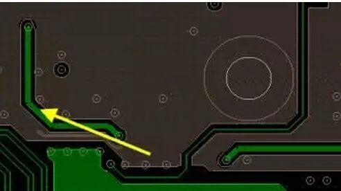
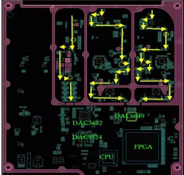
Layout Examples
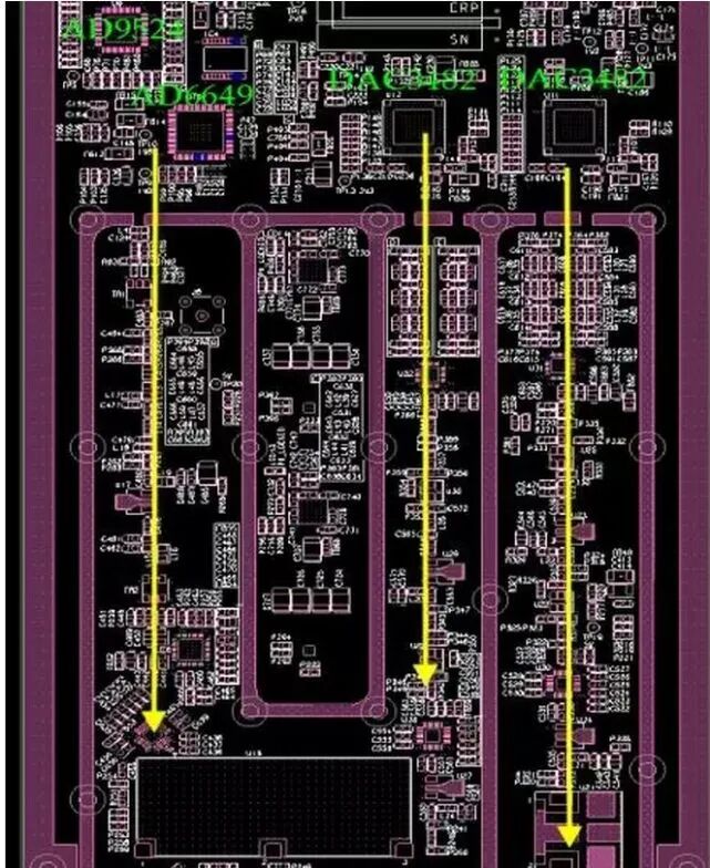
 Source: EDA365
· END ·
Follow the subscription account under EEWorld: "Automotive Development Circle"
Reply "DS" to receive the complete materials of "DeepSeek: From Beginner to Expert"

Scan to add the assistant and reply “Join Group”
Face-to-face communication with electronic engineers to exchange experiences