Definition of Impedance
In a circuit with resistance, inductance, and capacitance, the hindrance to the current in the circuit is called impedance.
Impedance is commonly represented by Z, which is a complex number. The real part is called resistance, and the imaginary part is called reactance. The hindrance caused by capacitance in the circuit to alternating current is called capacitive reactance, while the hindrance caused by inductance is called inductive reactance. The total hindrance caused by capacitance and inductance in the circuit to alternating current is collectively referred to as reactance.
The unit of impedance is ohms (Ω). Impedance includes resistance, inductive reactance, and capacitive reactance, and it is frequency-dependent.

Impedance Matching
When the internal resistance of the signal source is equal to the characteristic impedance of the transmission line and they are in phase, or when the characteristic impedance of the transmission line is equal to the load impedance and they are in phase, it is referred to as impedance matching at the input or output of the transmission line. 【Quoted from Baidu Encyclopedia】
Impedance matching is achieved by adjusting the input and output impedances to meet certain conditions, usually to maximize power transfer or minimize signal reflection.
In short, impedance matching is to ensure the stability and reliability of signal transmission. This is particularly crucial for high-speed signal lines, as they play a key role in the normal and stable operation of high-speed systems, thus impedance matching must be considered.
For more information, refer to PCB Hard Board Stack Design: Impedance Matching.
Factors Affecting PCB Board Impedance
-
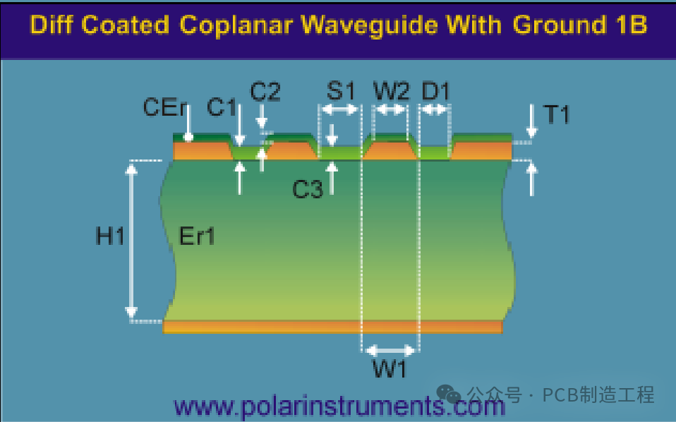
The thickness of the copper foil of the impedance line, such as T1; the thicker the copper, the lower the impedance value.
-
The width of the impedance line, where W1 is the width of the lower part of the impedance line and W2 is the width of the upper part; the narrower the line, the higher the impedance value.
-
The thickness of the dielectric layer between the impedance line and the reference layer or shielding layer, such as H; the thicker the dielectric layer, the higher the impedance value.
-
The dielectric constant, where Er is the dielectric constant of the dielectric layer and CEr is the dielectric constant of the solder mask ink; the lower the dielectric constant, the higher the impedance value.
-
The thickness of the solder mask ink, where C1/C3 is the thickness of the solder mask ink on the PP surface, and C2 is the thickness of the solder mask ink on the impedance line surface.
-
The distance from the impedance line to the adjacent copper foil, such as D1; the greater the distance, the higher the impedance value.
-
The distance between two differential impedance lines, such as S1; the greater the distance, the higher the impedance value.
Types of PCB Impedance
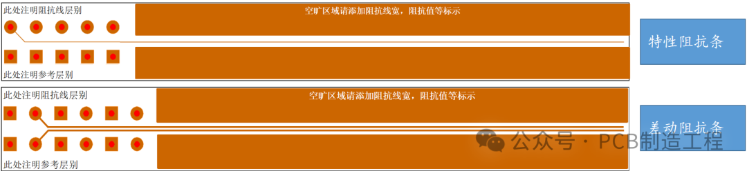
Characteristic Impedance
-
General/Standard Characteristic Impedance: The distance between the impedance line and the adjacent copper foil is irregular or there is no copper foil.
-
Co-planar Characteristic Impedance: The distance between the impedance line and the adjacent copper foil is regular.
-
Common characteristic impedance values: 45, 50, 55, 60 ohms.

Differential Impedance
-
General/Standard Differential Impedance: The distance between the impedance line and the adjacent copper foil is irregular or there is no copper foil.
-
Co-planar Differential Impedance: The distance between the impedance line and the adjacent copper foil is regular.
-
Common differential impedance values: 85, 90, 100, 110 ohms.

Impedance Testing
Impedance testing, simply put, is to determine whether the impedance of the signal line meets the expected impedance matching by testing the impedance value of the signal line.
PCB impedance testing is a routine testing method used to detect the impedance values of impedance lines (the lines that require impedance matching as per customer requirements) on PCB boards. PCB impedance testing can help ensure the performance of the PCB board under current and voltage conditions, and it can also verify whether the circuit design meets customer specifications.
1. Testing the impedance value of the impedance strip
-
The impedance strip is a coupon designed by the PCB manufacturer based on customer requirements (impedance line width, reference layer, type, etc.), combined with their own know-how and impedance testing equipment.
-
Coupon is a common term, and we can consider it as a PCB board designed by the PCB manufacturer.
-
Example of impedance strip: 2 test holes for characteristic impedance, 4 test holes for differential impedance.
2. Testing the impedance value of the impedance line within the PCB board
-
This method is limited by the design of the customer’s impedance line and the accuracy and hardware requirements of the testing equipment, such as the length of the impedance line, the size of the test pad, and the pitch of the pad.
3. Impedance Testing Instruments
-
Time Domain Reflectometry (TDR) is a commonly used PCB impedance testing method. It sends a short pulse signal to the transmission line on the PCB and then measures the reflection of this signal on the transmission line. By analyzing the amplitude and time delay of the reflected signal, the impedance characteristics of the PCB transmission line can be determined.

-
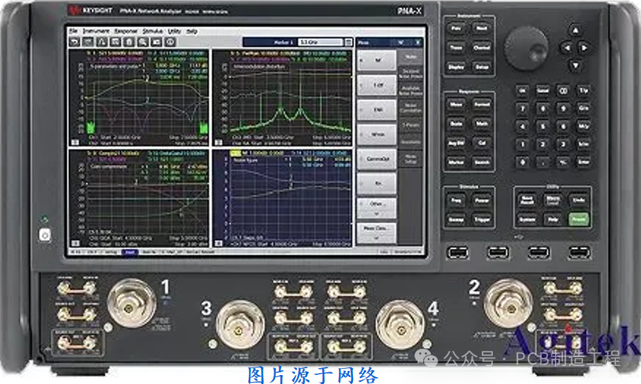
A Vector Network Analyzer (VNA) is an extremely precise instrument that characterizes the impedance of electrical networks. The measurement results can provide amplitude and phase details, allowing for a deeper understanding of their behavior. The Device Under Test (DUT) is typically used in RF applications, involving the response of individual components, cables, antennas, filters, amplifiers, etc.
In all cases, the VNA works by comparing its source signal with the measurements of reflected and transmitted signals to derive impedance and signal strength. The signal is compared to derive impedance and scattering parameters (S-parameters) data, allowing users to understand the power handling capabilities of the device.
The impedance measurement function is an important application of the VNA. VNA equipment is not very common in PCB manufacturing, so it will not be elaborated here. Interested readers can look up information related to VNA.
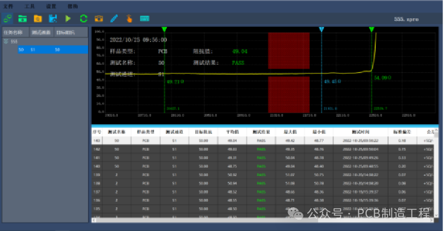
4. Why can’t the impedance testing range be the entire line segment but rather 30%~70%?
-
The contact of the probe at the front end with the impedance testing hole or pad has a certain degree of impact on the continuity of the impedance.
-
The end of the impedance coupon strip is in an open circuit state, which means infinite impedance, so the end impedance will be raised, affecting the actual impedance value. The impedance in the middle part will stabilize over time, and for the accuracy of the test, the relatively stable part in the middle is used to average the impedance value.
-
In summary, taking a middle range of 30%~70% or 50%~70% during testing is to reduce or eliminate the influence of the probe and open circuit at the front and back ends, thus avoiding the effects of the launch area and reflection area.
Supplement: For those interested in impedance optimization, you can refer to PCB Hard Board Impedance Optimization Discussion: Methodology and PCB Hard Board Impedance Optimization Discussion: Optimization Methods.