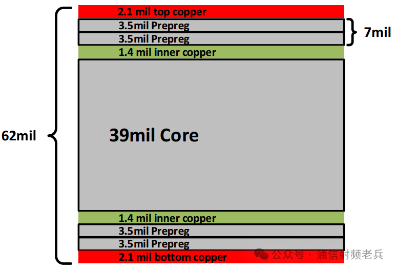
The following diagram shows a four-layer board, but the relevant content can also be applied to circuit boards with more layers. The core of a printed circuit board is a rigid fiberglass board, which is covered with copper foil on both the top and bottom. The core part is essentially a two-layer board. To increase the number of layers, a thin fiberglass sheet with adhesive, known as prepreg, is used to bond the copper foil on the top and bottom. This example printed circuit board shows a very common thickness. For instance, a 62mil thick circuit board is considered standard, and a 7mil thick prepreg is also quite common. Typically, the core part is relatively thick, while the prepreg is thin. Therefore, the top layer is very close to the top of the core part, and the bottom layer is close to the bottom of the core part.
To achieve good electromagnetic interference (EMI) performance, the signal layer should be as close as possible to its associated ground return layer. If the top layer is used as a signal layer and the adjacent inner layer is used as a ground return layer, this is a good choice because the prepreg is usually thin. To achieve good power decoupling, keeping the power layer and ground layer close together is also helpful. If the core part is used as the power layer and ground layer, it may be difficult to maintain a tight spacing because the material of the core part is usually thicker.
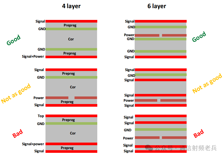
Here, we compare different stacking structures to see which is the best. The worst stacking structure is using two adjacent layers, each with signal traces. In this case, the two signals will interfere with each other, and the ground reference is usually far from the signal, causing the return current to spread out.
A common method used in four-layer boards is to use the power layer and ground layer as inner layers, while placing the signal layers on the outer layers. The power trace on the bottom will serve as the return path for the bottom signal. One potential issue with this method is that the power layer may be split into multiple power traces. In this case, discontinuities or gaps may appear in the return path, necessitating the use of stitching capacitors to bridge these gaps. Additionally, when signals transition from the top layer to the bottom layer, the return path needs to transition from the ground layer to the power layer, which may also lead to RF radiation.
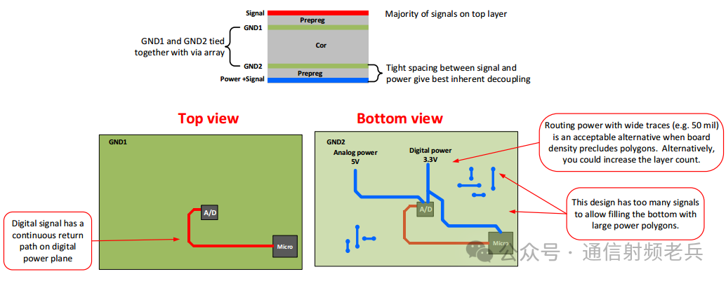
For four-layer boards, the best way to achieve good EMI performance is to use two inner layers as ground layers. In this case, signals will be distributed on the top layer, while power and signals will be on the bottom layer. The advantage of this method is that it allows the power traces to be very close to the ground return path, improving decoupling effectiveness. This method also eliminates the need for stitching capacitors, as the ground return is continuous and complete, whereas in the previous example, the power layer was split to accommodate multiple power traces. Furthermore, when signals on the top and bottom layers transition between different layers, the two ground layers are connected together through stitching vias, minimizing radiation.
Six-layer and higher printed circuit boards also follow the same principles. In short, you never want a signal layer without an adjacent ground return path. Additionally, keeping the power layer close to the ground layer will improve decoupling effectiveness.
 The following example illustrates how placing the power layer adjacent to the signal layer can cause problems. This method is not unworkable, but you must be careful to avoid routing signal traces over the split area of the power layer. In this example, the power is split into a 3.3V digital power plane and a 5V analog power plane. The design on the left will generate RF radiation because the digital signal traces cross over the split area in the return path. The layout on the right has been adjusted to maintain a continuous digital power plane beneath the digital input/output (I/O) lines. For this design, the return current will flow through the 3.3V digital power plane rather than the ground plane.
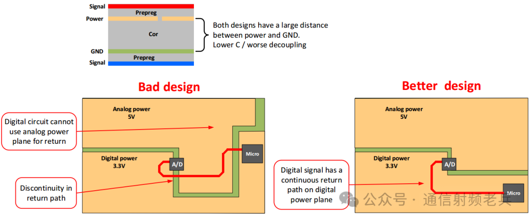
The diagram below shows how to use two inner layers as ground layers in a four-layer printed circuit board. In this case, most signals will be routed on the top layer, while the power layer will be on the bottom layer. The bottom layer can also route some signal traces, but most of the area on the bottom layer is dedicated to power. The advantage of this stacking structure is that it brings the power layer close to its ground return path, which will improve decoupling effectiveness due to the lower AC impedance between power and ground. Additionally, when signals transition between the top and bottom layers, there is no need to use stitching capacitors.
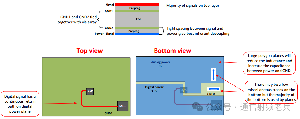
The example in the image above can be modified to route the power with thicker traces instead of a plane. If the transient current on the power trace is not very large, routing the power in trace form is a reasonable approach. Compared to using a power plane, this method has the advantage of providing more space on the bottom layer for routing signal traces.
 The following diagram is an example of a two-layer circuit board. For this type of circuit board, the best stacking method is to arrange the power and signals on the top layer and use the bottom layer as a complete ground plane. However, it is often difficult to route all signals and power traces on the top layer, so some traces are often routed on the bottom layer. So, what common problems might arise with this stacking method?
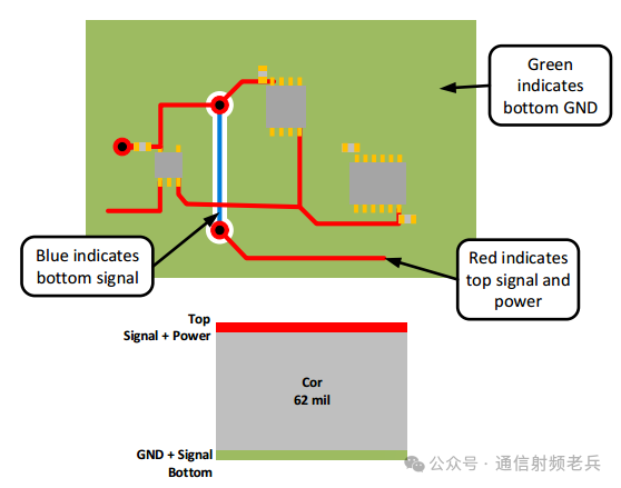
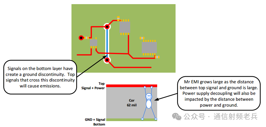
A significant problem with two-layer circuit boards arises because some traces need to be routed on the bottom layer. Traces on the bottom layer can lead to discontinuities in the ground path. When the signal from the top layer passes through this discontinuity, the ground return current has to bypass this split area, resulting in RF radiation.
Another problem arises because the top and bottom layers are physically separated by a considerable distance. The typical thickness of a two-layer circuit board is 62mil. This thickness is much greater than the distance between the top layer and the core layer in a four-layer board. Increasing the spacing between layers can cause the field distribution beneath the traces to spread out.
Remember the principles of electromagnetic interference (EMI). It propagates along the top and bottom of the waveguide. The spreading of the field distribution increases crosstalk between digital traces and sensitive analog traces. Of course, if the two-layer circuit board is made very thin, this problem can be minimized, but from a mechanical strength perspective, this may not be very practical.
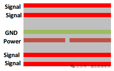
 Tips: Common questions and answers about PCB stacking selection1. What potential problems exist with the following stacking structure?
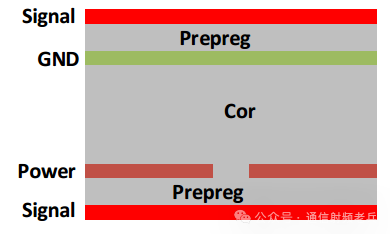 a) To achieve good shielding, the ground layer should always be at the bottom.
b) The power layer should never be split.
c) The power layer and ground layer are too far apart. This will reduce high-speed decoupling performance.
d) The power layer is split, so signals crossing the split area on the bottom layer may have RF radiation issues.
e) Answers a and b are problems.
f) Answers c and d are problems.
Answer:The correct answer is “f”, meaning that answers c and d are problems. Keeping the ground layer and power layer close together can reduce the high-frequency impedance between layers. This low impedance can eliminate power noise. In this case, the power layer and ground layer are far apart, so high-speed decoupling performance will decrease.
Additionally, the power layer is split. If signal traces cross this split area, this division can cause issues.
2. What potential problems exist with the following stacking structure?
a) Two adjacent signals do not have adjacent ground return paths, so they may interfere with each other.
b) The ground layer and power layer are too close together; they should be separated further to prevent power noise from coupling into the ground layer.
c) None of the above are problems; this is a good stacking structure.
Answer:The correct answer is “a”, meaning that two adjacent signals do not have adjacent ground return paths, so they may interfere with each other. In this case, the signals on the top two layers will reference the ground plane, and all return currents will mix, causing crosstalk. On the bottom two layers, the signals reference the power plane, and similarly, the return currents will mix. Additionally, the bottom layer has a split condition, and if signals cross this split area, this may also cause issues.