
Metal halide perovskite materials (MHPS) exhibit excellent optoelectronic properties and have broad application prospects in fields such as photovoltaics, light-emitting diodes, and lasers. A key step to fully exploit the potential of these materials is to achieve high-resolution, top-down patterned large-scale chip integration. Developing such a patterning method for perovskite films is challenging due to the inherent ionic nature of perovskite thin films and their adverse reactions with solvents used in standard photolithography processes.
AMO GmbH Max C. Lemme and Maryam Mohammadi and others introduced a universal and precise method that includes photolithography and reactive ion etching (RIE) processes, which can be adjusted to accommodate different perovskite compositions and morphologies. By utilizing traditional photoresists at lower temperatures, micron-sized features with a precision of 1 μm can be produced with high reproducibility. The patterning technique was validated using atomic force microscopy (AFM), X-ray diffractometry (XRD), spectroscopic analysis, and scanning electron microscopy (SEM).
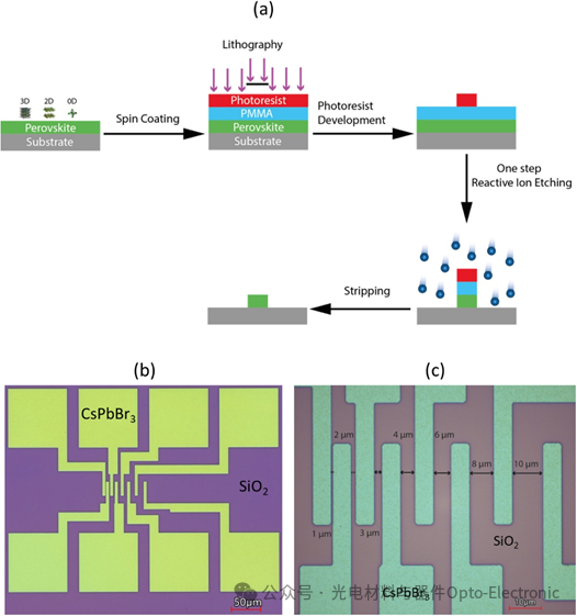
Figure 1.(a) The manufacturing process includes the following steps: (1) Deposit the perovskite thin film (3D, 2D, or 0D), (2) Deposit a PMMA layer and a photoactive resist layer (AZ Mir 701), (3) Develop the AZ Mir701 resist layer, (4) Transfer the pattern to the perovskite layer via reactive ion etching, and (5) Strip by dissolving the bottom resist layer. (b, c) Optical microscope images of device features obtained through the top-down patterning method.
The advantages of this strategy include: 1. A dual-stack photoresist design using polymethyl methacrylate (PMMA) and commercial positive photoresist AZ MIR 701 in a bilayer structure, where the PMMA layer isolates the perovskite from direct contact with the photoresist, avoiding chemical damage, while AZ MIR 701 ensures compatibility with standard photolithography processes. 2. Oxygen-free etching optimization: Custom etching gases for different types of perovskites: Inorganic perovskites (e.g., CsPbBr3) use HBr and BCl₃ radicals, while organic-inorganic hybrid perovskites (e.g., MAPbI3) use CF₄, Cl₂ mixed with He gas, while controlling substrate temperature through an “etch-wait” cycle to avoid high-temperature damage. This technology can achieve a minimum feature size of 1μm, with high reproducibility between chips, and is compatible with 3D (e.g., CsPbBr3, MAPbI3), quasi-2D (PEA₂(MAPbBr3)n-1PbBr4), and 0D (FAPbI3 nanocrystals) and other multi-dimensional perovskite materials.
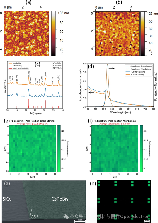
Figure 2. CsPbBr3 patterning (a) Atomic force microscopy scan of the original sample. (b) Atomic force microscopy scan after etching and stripping the dual-layer stack. (c) X-ray diffraction patterns of the sample before and after etching. (d) UV-Vis spectra and PL spectra before and after etching. (e, f) Comparison of photoluminescence peak positions before and after etching over an area of 25 μm×25 μm. (g) Cross-sectional scanning electron microscopy image of the etched structure. (h) Confocal fluorescence microscopy image of the etched structure array.
AFM observations revealed that after etching, the RMS roughness of the CsPbBr3 thin film increased, with larger particle sizes, more pinholes, evidence of recrystallization, and a reduction in the second phase. XRD confirmed no significant differences in crystal phases before and after etching, primarily consisting of CsPbBr3 phase. UV-Vis and PL spectra showed that the optical properties were largely preserved before and after etching, with a slight increase in photoluminescence quantum yield. SEM and other analyses showed low edge roughness and clear structures of the etched features. This method is applicable to various fully inorganic perovskite materials, indicating its potential in device applications.
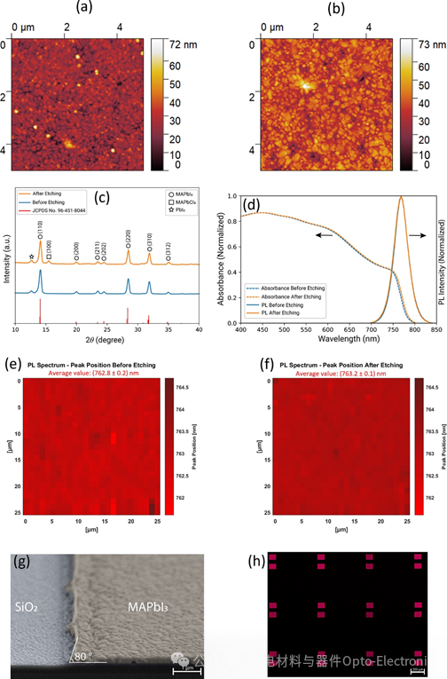
Figure 3 MAPbI3 patterning (a) Atomic force microscopy scan of the original sample. (b) Atomic force microscopy scan after etching and stripping the dual-layer stack. (c) X-ray diffraction patterns of the sample before and after etching. (d) UV-Vis spectra and PL spectra before and after etching. (e, f) Comparison of photoluminescence peak positions before and after etching over an area of 25 μm×25 μm. (g) Cross-sectional scanning electron microscopy image of the etched structure. (h) Confocal fluorescence microscopy image of the etched structure array.
Research on the etching of the organic-inorganic hybrid perovskite MAPbI3 found that AFM showed a slight increase in surface roughness, with no significant changes in grain size. XRD indicated different compositions at the edges of the patterned areas due to halide exchange, forming MAPbI3-xClx. UV-Vis and PL spectra showed stability in the central region, with a blue shift of 7 nm at the edges. PLQY decreased from 0.213% to 0.172%. SEM showed sidewall angles of approximately 80°, enabling the fabrication of various patterns.
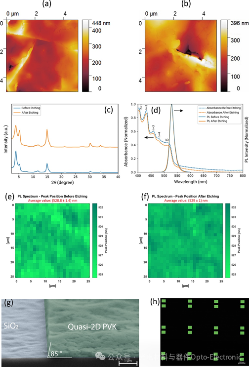
Figure 4. PEA₂(MAPbBr3)n-1PbBr4 quasi-2D perovskite patterning. (a) Atomic force microscopy scan of the original sample. (b) Atomic force microscopy scan after etching and stripping the dual-layer stack. (c) X-ray diffraction patterns of the sample before and after etching. (d) UV-Vis spectra and PL spectra before and after etching. (e, f) Comparison of photoluminescence peak positions before and after etching over an area of 25 μm×25 μm. (g) Cross-sectional scanning electron microscopy image of the etched structure. (h) Confocal fluorescence microscopy image of the etched structure array.
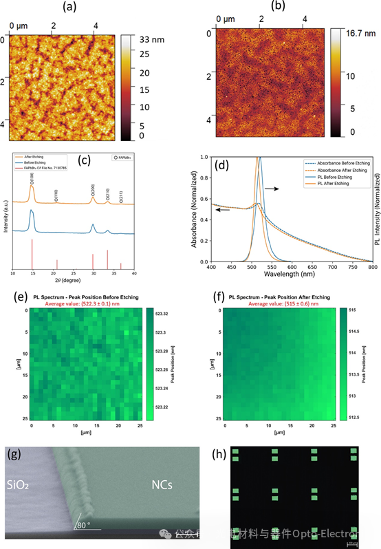
Figure 5. FAPbBr3 patterning (a) Atomic force microscopy scan of the original sample. (b) Atomic force microscopy scan after etching and stripping the dual-layer stack. (c) X-ray diffraction patterns of the sample before and after etching. (d) UV-Vis spectra and PL spectra before and after etching. (e, f) Comparison of photoluminescence peak positions before and after etching over an area of 25×25 μm. (g) Cross-sectional scanning electron microscopy image of the etched structure. (h) Confocal fluorescence microscopy image of the etched structure array.
Summary: Based on traditional photolithography and reactive ion etching, researchers have developed a top-down patterning technique for metal halide perovskites. This method has been demonstrated on organic-inorganic hybrid compounds and various dimensional (3D, 2D, and 0D) fully inorganic compounds. The technique was evaluated using atomic force microscopy, X-ray diffractometry, optical spectroscopy, and scanning electron microscopy, confirming that aside from the edges of the patterned organic-inorganic metal halide perovskites, the phase and optical properties of the perovskites were not significantly affected by the patterning process. The organic metal halide perovskite MAPbI3 experienced local halide exchange with etching gas ions at the edges of the patterned areas, which can be explained by its inherent soft lattice crystal structure. The developed microstructuring technique showed reproducible results with a resolution of 1 μm, sufficient for future potential industrial applications integrating perovskites. The UV photolithography combined with a single-step RIE developed in this work provides a good balance between resolution, material compatibility, scalability, and industrial feasibility. The proposed method is suitable for wafer-scale applications and can utilize higher resolution photolithography tools for high throughput and smaller sizes. Therefore, it can integrate different types of metal halide perovskite wafers onto chips using industrial standard processes. This technology enables flexible device engineering and can accelerate research and development in perovskite-based optoelectronics, electronics, and energy harvesting applications.
Article Information:
Title: A Versatile Top-Down Patterning Technique for Perovskite On-Chip Integration
Authors: Federico Fabrizi, Saeed Goudarzi, Sana Khan, Tauheed Mohammad, Liudmila Starodubtceva, Piotr J. Cegielski, Felix Thiel, Sercan Özen, Maximilian Schiffer, Felix Lang, Peter Haring Bolívar, Thomas Riedl, Gerhard Müller-Newen, Surendra B. Anantharaman, Maryam Mohammadi,* and Max C. Lemme*
Original Link:
https://doi.org/10.1021/acsnano.5c10397
Note: This article is originally written by the optoelectronic materials and devices team, aiming to share relevant research knowledge. Due to limited knowledge, there may be omissions and errors, and scholars and colleagues are welcome to provide feedback and corrections.
This article is for academic sharing and communication only. If there is any infringement, please contact the administrator for deletion.
Submissions for sharing and communication are welcome, email: [email protected]