Click the blue text
Follow us
Chips, as the “brain” of modern technology, are ubiquitous from smartphones to aerospace satellites. But did you know? This precision device, the size of a fingernail, originates from unassuming quartz sand. Today, we will unveil the mystery of chip manufacturing and see how it transforms from “sand” into the “intelligent core” step by step.
1
Division of Labor in Chip Manufacturing: Who is “Building Blocks”?
Chip manufacturing is a “super project” that requires global collaboration. The main division of labor includes:
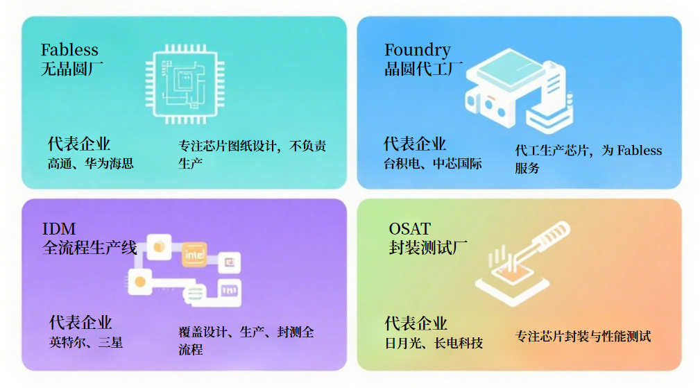
●Fabless (without a foundry): Focuses on design, such as Qualcomm and Huawei HiSilicon, and does not handle production.
●Foundry (wafer foundry): Contract manufacturing, such as TSMC and SMIC, produces chips for Fabless companies.
●IDM (Integrated Device Manufacturer): Covers the entire process of design, production, and testing, such as Intel and Samsung.
●OSAT (Outsourced Semiconductor Assembly and Test): Focuses on chip packaging and testing, such as ASE and JCET.
2
Wafer Preparation: How is the “Foundation” of Chips Made?
The wafer is the “foundation” of the chip, made from high-purity silicon. Its preparation process is akin to “alchemy”, with precision at every step:
1. From Quartz Sand to Electronic-Grade Silicon: Purity 99.9999999%!
●Raw Material: Quartz sand (silicon dioxide) → reacts with carbon to produce metallurgical-grade silicon (purity 98%) → purified through chlorination and distillation to obtain electronic-grade silicon (9~11 nines purity), purer than gold!
●Comparison: The photovoltaic industry uses “solar-grade silicon” (4~6 nines), while chips require higher purity.
2. Pulling Monocrystalline Silicon: “Growing” Perfect Crystals
●Polycrystalline Silicon → Monocrystalline Silicon: Polycrystalline silicon has an irregular structure and must be made into monocrystalline silicon using the Czochralski method.
Process: Melt polycrystalline silicon → insert seed crystal (monocrystalline silicon “nucleus”) → rotate and pull → form cylindrical silicon ingots (crystal rods), with a diameter of up to 30 cm and a length of 1~1.5 m.
●Key: Temperature and pulling speed must be precisely controlled; otherwise, crystal defects will occur.
3. Cutting, Grinding, Polishing: From “Silicon Rod” to “Mirror-like Thin Slice”
● Cutting: Silicon ingots are cut into silicon wafers (e.g., 12-inch wafers) with a thickness of 0.775 mm, using diamond wire saws or inner circular saws, with micron-level precision.
●Beveling + Grinding + Polishing:
Beveling: Rounding the edges of the silicon wafer to prevent chipping;
CMP (Chemical Mechanical Polishing): Using chemical etching + mechanical grinding to make the surface smooth as a mirror, paving the way for subsequent processes.
4. Wafer Trivia: Why are they round? Are they always made of silicon?
●Reason for Round Shape: The cylindrical shape is naturally formed during crystal pulling, and cutting results in a round shape; heating and cooling are more uniform, maximizing area utilization.
●Diverse Materials: Silicon accounts for over 90%, but there are also semiconductor materials like GaAs (second generation), GaN/SiC (third generation, used for fast charging, 5G), and diamond (fourth generation).
3
Chip Manufacturing (Front-End Process):
Layered “Nano-level Architecture”
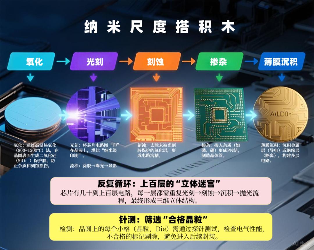
Once the wafer preparation is complete, it enters the core stage of chip manufacturing —the front-end process. This step involves hundreds of processes such asoxidation, photolithography, etching, doping, deposition, each akin to “building blocks” at the nanoscale.
1. Oxidation: Giving the Wafer a “Protective Coat”
●Purpose: To generate a silicon dioxide (SiO₂) protective film on the wafer surface to prevent impurities and etching damage.
●Process: High-temperature thermal oxidation (800~1200℃), with dry (pure oxygen) and wet (oxygen + steam) methods; dry method is more commonly used.
2. Photolithography: The “Blueprint Printing” of Chips
●Core: To “print” the chip circuit diagram onto the wafer, akin to “nanoscale printing”.
●Steps:
Coating: The wafer is coated with photoresist (light-sensitive material), with positive resist dissolving easily when exposed to light, and negative resist doing the opposite.
Exposure: The photolithography machine uses a mask (glass plate containing the circuit pattern) and irradiates the photoresist with ultraviolet (DUV) or extreme ultraviolet (EUV) light to “draw” the circuit.
Development: Dissolving the exposed photoresist, leaving the circuit pattern.
●Key Equipment: EUV lithography machine (extreme ultraviolet light, wavelength 13.5nm), produced only by ASML, with a single unit costing over $100 million!
3. Etching: “Digging Holes” to Form Circuit Trenches
●Purpose: To remove the oxide layer not protected by photoresist, forming circuit trenches.
●Process:
Dry Etching (mainstream): Uses plasma bombardment to vertically “dig holes” with high precision;
Wet Etching: Uses chemical solutions to dissolve, isotropic (spreading in all directions), suitable for non-critical layers.
4. Doping: “Injecting Soul” into the Silicon Wafer
●Purpose: Pure silicon is non-conductive and needs to be doped with impurities (such as phosphorus, boron) to form PN junctions and create transistors.
●Process: Ion implantation (high-energy particle beams inject impurities into the silicon wafer), forming N wells (containing electrons) or P wells (containing holes), constructing the “switch” structure of transistors.
5. Thin Film Deposition: Layering the “Circuit Network”
●Purpose: To deposit metal layers (conductive) or insulating layers (isolation), constructing multi-layer circuits.
●Process:
CVD (Chemical Vapor Deposition): Generates insulating films (such as silicon dioxide) through chemical reactions;
PVD (Physical Vapor Deposition): Sputters metals (such as copper, aluminum) in a vacuum environment to form conductive lines;
ALD (Atomic Layer Deposition): Stacks single atomic layers, precisely controlling thickness (at the nanoscale).
6. Repeated Cycles: A “3D Maze” of Hundreds of Layers
Chips have dozens to hundreds of layers of circuits, and each layer requires repeating thephotolithography → etching → deposition → polishing process, ultimately forming a three-dimensional structure.
7. Probing: Screening “Qualified Chips”
●Testing: Each small grid (chip, Die) on the wafer must pass probe testing to check electrical performance; unqualified ones are marked for removal to avoid entering subsequent packaging.
Conclusion

From quartz sand to chips, it undergoes thousands of processes, involving extreme challenges in materials, equipment, and technology. This is not only a crystallization of technology but also a result of global collaborative wisdom. The next time you pick up your phone, will you think of the trillion transistors “inside” it, working silently with nanometer-level precision?
END
Disclaimer
The content of this article is compiled from public information, aimed at information sharing, maintaining a neutral stance.
The images used in this article are AI-generated. If there are any infringement issues, please contact us promptly, and we will handle or delete them as soon as possible. Thank you for your understanding!
More Communication
//
If you want to join the relevant WeChat discussion group, you can add the editor “Xiao Ming” on WeChat.

Note: When adding “Xiao Ming”, please specify your real name + company + position
 Cooperation Consultation
Teacher Gu:137 7157 5253
Teacher Qiu: 158 6155 3579
Address:4th Floor, Building 8-1, Shanshui City Industrial Park, Binhu District, Wuxi City, Jiangsu Province
Website:www.cali-light.com
Disclaimer: The content of the article is aimed at information sharing, maintaining a neutral stance. If there are any infringement issues, please contact us promptly, and we will handle or delete them as soon as possible. Thank you for your understanding!


