This article is authorized to be reproduced from the public account “Semiconductor Industry Observation”, ID: icbank, Author: Du Qin
Today, almost everyone knows about lithography machines; the most advanced EUV lithography machines are as tall as a new Boeing jet. In the development history of lithography machines, various manufacturers from different countries have emerged, the US invented the technology, Japan promoted it, and the Netherlands became the ultimate winner.Today, we will discuss how the US, as the inventor of lithography technology, gradually lost this critical aspect of semiconductor manufacturing. The research on US lithography technology began at Bell Labs, improved by Fairchild, then GCA became the first company to manufacture stepper equipment, followed by the continuous development of Cobilt and P-E companies, until the last US lithography company SVG was acquired by ASML. One by one, early companies were acquired, divested, or dissolved, and the US gradually lost the opportunity to own lithography machines.
Started at Bell Labs
As early as the mid-1950s, Bell Labs began to experiment with printing images onto silicon wafers. In 1955, Jules Andrus and Walter L. Bond at Bell Labs began to use existing lithography (also known as photolithography) technology to create patterns on printed circuit boards, using the silicon dioxide layer from Frosch and Derick to produce finer and more complex designs on the silicon wafer. A photosensitive coating or “photoresist” was applied to this layer, and the desired pattern was exposed to this layer through an optical mask, then the unexposed photoresist was washed away, determining the precise window area through chemical etching. Impurities diffused into the underlying silicon through these openings, forming the n-type and p-type silicon regions required for semiconductor devices.In 1957, Jay Lathrop and James Nall from the US Army Diamond Ordnance Fuse Laboratory obtained a patent for lithography technology during their early attempts to miniaturize electronic circuits, which was used to deposit thin metal strips about 200 microns wide to connect discrete transistors on ceramic substrates. They also used this technology to etch holes in silicon dioxide to create diode arrays. In 1959, Lathrop joined Texas Instruments while Nall went to Fairchild. Following this pioneering work, Jay Last and Robert Noyce manufactured one of the first “step-and-repeat” cameras at Fairchild in 1958, utilizing lithography technology to produce many identical silicon transistors on a single wafer.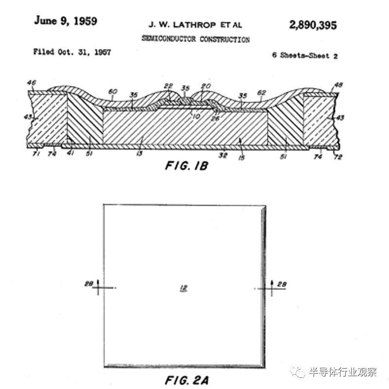 Semiconductor manufacturing patent by Lathrop et al.(Source: US Patent Office)
The Rise and Fall of Lithography Pioneer GCA
GCA is known as a pioneer in important chip manufacturing technology for lithography. On this day in 1959, GCA acquired David W. Mann. In 1961, GCA’s David W. Mann division became the first company to manufacture commercial step-and-repeat and photoreduction equipment (photo-repeaters). The photorepeater is the predecessor of the wafer stepper.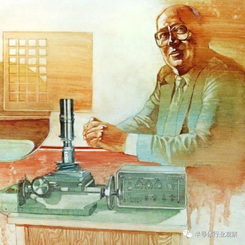 Burt Wheeler developed the Mann photorepeater for mask manufacturing(Source: Semiconductor Equipment and Materials International)In 1975, GCA introduced the first wafer track for photoresist processing. In 1978, GCA launched the DSW 4800, the first successful wafer stepper (g-line, 10X, Zeiss 0.28NA lens, 10mmX10mm size), priced at $450. GCA’s early customers included IBM, ATT, Fairchild, National Semiconductor, and Siemens. Although the actual release was in ’78, the test tools were delivered to IBM in ’77. The stepper revolutionized semiconductor patterning, showing lower defect rates, significantly better coverage performance, and better yields. However, compared to the projection aligners from Perkin Elmer (mentioned later), its throughput was lower. The generation of 256K DRAM truly made the stepper a mainstream lithography tool.However, in 1980, Nikon launched Japan’s first commercial stepper, the NSR-1010G. Nikon’s success outperformed GCA. Nikon attracted customers by producing lenses with higher resolution than GCA. Nikon achieved a resolution of 1µm with a 5x reduction instead of 10x. With this stepper, machines were no longer “slow”. GCA tried to keep up with this development, but Zeiss was their only lens supplier, making it difficult for them to stock enough materials in time. Thus, GCA experienced delays in delivering competitive tools. GCA’s market share in Japan’s stepper market dropped from about 68% in 1981 to around 45% in 1983.In 1982, GCA purchased the Tropel lens manufacturing unit from Coherent Laser. In 1985, they developed the first DUV stepper for Bell Labs. “GCA spent $5 million developing the first g-line stepper. The development cost for their i-line stepper was $25 million, and the DUV stepper cost $140 million,” Neil Bonke stated at the 1988 SEMI Industrial Strategy Symposium (ISS).
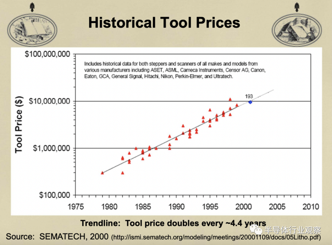 Prices of early lithography tools(Source: Sematech)From 1985 to 1986, GCA lost $100 million in two years, laying off 70% of its workforce, reducing to only 1,000 employees. In 1988, General Signal acquired the financially troubled GCA for $76 million. Subsequently, Sematech funded GCA to develop KrF steppers. In January 1993, General Signal announced its intention to divest its semiconductor equipment company. In May 1993, due to the inability to find a buyer, General Signal shut down GCA. These intellectual properties were transferred to Integrated Solutions Inc. (ISI), which was later acquired by Ultratech in 1998. Thus, the chapter of GCA, a pioneer of lithography technology, was turned.
Cobilt Pushed Off the Historical Stage by Perkin-Elmer
Another American lithography company to mention is Cobilt. Before discussing Cobilt, there is much background to consider. In the 1960s, contact printing was the main technology for exposing patterns on IC wafers. In the early ’60s, chip manufacturers began making their own equipment. Kulicke & Soffa (K&S) was the first company to sell commercial tools. They were very successful, capturing almost 100% of the market share in the ’60s (albeit small). In 1970, K&S collaborated with Computervision to develop the first automatic aligner, showcased at the WESCOM exhibition. After selling over 50 units, K&S lost interest in the venture and exited the industry.Later, Kasper Instruments became the main supplier of contact aligners, capturing about half of the market by 1973. Contact aligners were simple and quick to use but required direct contact between the mask and wafer, which could damage the mask or contaminate the wafer. To solve these issues, proximity aligners were introduced in 1973. By 1974, nearly half of the aligners sold by Kasper had this capability, but due to usability issues and competition from Canon, sales steadily declined, leading the company to exit the industry in 1981.Then three engineers from Kasper Instruments went out to establish a company manufacturing contact printers called Cobilt. After 1970, Cobilt developed lithographic wafer track technology, but the track business was eventually sold to Japan’s Tokyo Electron Ltd., which became the origin of Tokyo Electron’s track.Cobilt also manufactured mechanical aligners, which had better technology for printing semiconductor wafers than the standards at the time, and the machine featured an automatic alignment package for more precise layer alignment. Hundreds of these machines were sold worldwide until projection printing aligners took over the market.After Cobilt came Perkin-Elmer (P-E), whose rise also defeated Cobilt. In 1973, Perkin-Elmer launched the microralign projection scanner, a result of an early Air Force research contract. When the mask aligner transitioned from contact mask aligners to projection aligners, which projected the mask’s image onto the wafer, P-E completely dominated this market. In 1979, the microralign was priced at $170,000 and sold over 2,000 machines. In 1981, P-E announced that the Micralign 500 projection machine could produce 100 wafers per hour, priced at $675,000.Cobilt attempted to build a projection printing aligner but failed. In 1981, Cobilt’s lithographic exposure tool business was acquired by Applied Materials, which hoped to add lithography tools to their product lineup but ultimately disbanded the Cobilt division.By the late 1980s, the dominance of Japanese stepper suppliers became evident, causing concern among US chip manufacturers. To develop alternatives to lithography, Intel collaborated with a European company, Censor, but manufacturing steppers was very complex and expensive, and the development speed was too slow. Meanwhile, Canon and Nikon’s steppers performed well, with no comparable equipment available in the US, leading Intel to eventually purchase Japanese equipment. Censor was also sold to Perkin-Elmer in 1984.In April 1989, P-E announced its exit from the semiconductor equipment business. With investments from IBM and five other companies, P-E divested its electron beam lithography department Etec. Next came the story of SVG.
Finally SVG
In the 1990s, Silicon Valley Group (SVG) expanded into the lithography field under the leadership of newly appointed CEO Papken Der Torossian. SVG attempted to acquire GCA, but the deal fell through. However, SVG successfully acquired P-E’s lithography business, jointly developed with IBM, the next-generation step-and-scan system Micrascan for $20 million in 1990. With negotiations pushed by HP and Nikon, IBM also made a 15% financial investment in P-E.But SVG’s Der Torossian stated that it would take tens of millions of dollars in R&D funding and two and a half years to fix the errors in the system. “Their machines couldn’t work, with an average mean time between failures of less than an hour. IBM couldn’t use it. But it had very good foundational technology.”From 1990 to 1993, the Sematech consortium spent about $30 million helping SVG develop Micrascan. In 1990, the industry’s first step-and-scan tool, Micrascan, was launched. In June 1992, Micrascan II was introduced. In 1993, SVG intended to discuss sharing step-and-scan technology with Canon. However, due to pressure from the US government, technology transfer to Japan was not allowed, and negotiations ended after a year. However, during 1991-1994, it sold fewer than 10 units each year.In 1996, SVG launched Micrascan III, which could switch to excimer laser sources, with NA ranging from 0.4 to 0.6. In 1999, Micrascan 193 tools (NA = 0.6) were introduced. Intel, Motorola, and Texas Instruments invested a total of $30 million in SVG in 1995 to accelerate the development of this tool. Micrascan III, along with subsequent models IV and V, sold around 50 units annually, allowing SVG to survive for a while.In 1980, US suppliers held 90% of the litho tool market share. By 1990, it had dropped to 10%. GCA and Ultratech each held about 4-5%, while SVG had about 1%. They were even falling behind the latest competitor, ASML.According to SemiWiki, in 1992, ASML, then under Philips, was seeking a buyer. At that time, Philips approached SVG’s Der Torossian, wanting to sell ASML for $60 million, but SVG did not have that much cash and hoped to establish a joint venture through equity, while Philips needed cash. The lack of cash led to the US losing the opportunity to retain advanced lithography technology.In October 2000, the tide turned when ASML announced its intention to acquire SVG for $1.6 billion, as ASML needed the refractive index and CaF technology for 157nm lithography. Ultimately, in May 2001, ASML successfully acquired SVG Lithography. In November 2001, SVG’s Micrascan 248nm and 193nm tools were discontinued. The last major lithography company in the US came to an end.
Conclusion
The decline of the US in lithography technology was met with resistance from Japan’s Nikon and Canon, but no one expected that it was a lithography machine that ASML had devoted decades to research, now unmatched by anyone.
Editor: Southern Cat