 👆If you would like to meet regularly, feel free to star 🌟 and bookmark it~Source: ContentTranslated fromthebrighterside, thank you.
From online shopping to medical research, artificial intelligence (AI) continues to impact our daily lives. However, behind every click or discovery lies a world of computational power facing significant challenges. Today’s computers consume vast amounts of energy and generate heat, limiting their speed and efficiency. To address these issues, researchers have found an unexpected solution: computing with light instead of electricity.
German tech company Q.ANT’s recent breakthrough promises to redefine the production of AI chips, leading to faster, more environmentally friendly, and more powerful computers worldwide.
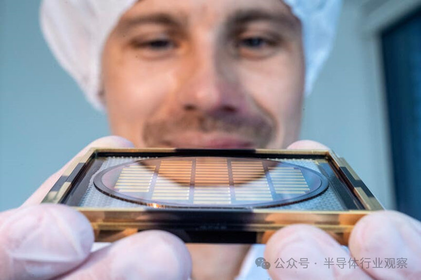
In a high-tech factory in Stuttgart, engineers have launched an advanced production line specifically for manufacturing photonic AI chips. These chips utilize thin-film lithium niobate (TFLN), a special material well-suited for managing optical signals. This material can control light waves very quickly without generating excessive heat.
By upgrading existing semiconductor factories, the new method significantly reduces costs and accelerates the development of AI processors. This €14 million investment in innovative technology is expected to reshape the global chip manufacturing industry, setting an example for other countries to enhance their technological production capabilities.
According to Dr. Michael Förtsch, CEO of the company, this technology sets a new benchmark for “AI chip manufacturing,” aiming to improve energy efficiency and independence in semiconductor production.
Photonic chips, also known as photonic neural processing units (NPU), are cutting-edge processors that compute using light rather than electricity. Unlike traditional electronic chips that rely on electrons moving through metal wires, photonic chips manipulate photons (particles of light) through waveguides, modulators, and other optical components etched onto silicon substrates.
This medium shift allows photonic NPUs to execute certain computations faster and more efficiently than traditional processors, especially those related to artificial intelligence (AI) and neural networks.
The core of the photonic NPU is the concept of light interference. Light waves can combine or cancel each other based on their phase and amplitude, a property that can be used to perform matrix multiplication—the core operation in AI workloads.
For example, when light passes through a programmable interferometer network, it can be configured to represent the weight matrix used in neural networks. The interference pattern results at the output corresponds to the computed data, effectively executing complex calculations at the speed of light.
One significant advantage of photonic chips is their ability to process multiple data streams simultaneously through wavelength division multiplexing technology. Each wavelength (or color) of light can carry its own information stream, enabling high-throughput parallel processing without being affected by the thermal and electrical performance limitations of traditional chips. This means photonic NPUs can achieve extremely high bandwidth and lower latency while consuming less power.
Additionally, photonic chips are inherently suitable for analog computing. Unlike digital electronic devices that break information down into bits, photonic systems can represent and manipulate continuous values, which is very useful for tasks like signal processing and AI inference. However, this also presents a challenge: maintaining precision and managing noise in analog optical systems is very difficult, so hybrid designs integrating both photonic and electronic components are often employed.
Photonic chips can increase processing speeds by 50 times while reducing energy consumption by 30 times. This means data centers, which are crucial for managing large-scale computational tasks, can operate faster and more sustainably.
Dr. Förtsch emphasized the urgent need for this transformation, stating, “As AI and data-intensive applications push traditional semiconductor technology to its limits, we need to rethink how core computing is done.” Photonic processors provide such a solution, offering a sustainable approach that meets the growing computational demands without placing excessive strain on existing infrastructure.
One major advantage of photonic chips is their ability to execute extremely fast light signal adjustments at thousands of gigahertz frequencies. Since these adjustments generate almost no heat, they operate more accurately and efficiently than traditional silicon chips. This efficiency is crucial for modern AI systems, as tasks like machine learning, scientific simulations, and real-time data analysis require extensive mathematical computations.
Professor Jens Anders, CEO of the semiconductor research institute responsible for the new production line, emphasized that the new photonic chips set the blueprint for “energy-efficient next-generation computing.” He highlighted that now is the best time for such technologies, as the rapid development of AI and its related applications will soon pose a significant threat to traditional data centers.
Beyond laboratory experiments, photonic chips have demonstrated their potential through cloud-based AI trials. These processors can be seamlessly integrated into existing data centers via standard PCIe interfaces, enhancing current computational configurations. They can efficiently handle critical AI workloads, such as model training, complex simulations, and the high-density mathematical operations required in machine learning applications.
This technology is not intended to replace traditional processors like GPUs (graphics processing units) but to complement them, just as GPUs currently supplement standard CPUs (central processing units). “We are not looking to replace GPUs but to reshape the next-generation computing ecosystem,” Dr. Förtsch explained, emphasizing that photonic technology will become the future standard for AI co-processors.
The production line can currently process up to 1,000 wafers per year, supporting the continuous development and fine-tuning of chip designs. The facility also serves as a research center for advanced server technologies designed for high-performance computing environments. Engineers and researchers can quickly adjust chip architectures to meet the ever-changing market demands, significantly accelerating the process from lab to market.
Six years ago, the team behind this innovation bet on TFLN technology. Today, that decision has yielded significant advantages. Their expertise in photonics, along with comprehensive control over the manufacturing process from raw materials to finished products, has positioned them uniquely in the semiconductor industry. This also marks a critical step toward achieving widespread applications and economic viability for high-speed, low-energy computing.
Establishing a blueprint for photonic chip production offers benefits that extend beyond a single region or company. It provides a model for other countries committed to strengthening their semiconductor industries. Currently, global semiconductor production heavily relies on a few key regions. Any disruption could have severe consequences, affecting various fields from automotive manufacturing to critical medical technologies.
This new method of photonic chip production helps reduce dependence on global supply chains. Countries adopting similar manufacturing methods can produce their own advanced processors, enhancing their resilience against future disruptions. This strategy offers a practical pathway toward a more distributed and stable semiconductor industry.
The company’s ultimate goal is ambitious yet clear: by 2030, to make photonic processors a vital component of global AI infrastructure. “By 2030, our goal is to make our photonic processors the scalable, energy-efficient cornerstone of AI infrastructure,” Dr. Förtsch stated, emphasizing a long-term commitment to sustainably reshaping technology.
The computing field is set to undergo transformative impacts. Data centers will become cooler, faster, and operational costs will significantly decrease. Scientific research and industry applications will accelerate, driving innovations in medicine, climate modeling, and robotics at unprecedented speeds.
This breakthrough is not merely an incremental improvement but a significant shift. Photonic processors harness the power of light, promising substantial gains in speed, efficiency, and sustainability. They represent not only more advanced technology but also smarter technology, perfectly aligned with an AI-driven future.
With photonic computing, the bottlenecks of traditional chips may soon become a distant memory. As this technology scales and becomes mainstream, the possibilities for innovation will be boundless. AI-driven industries, research institutions, and even your personal tech devices may soon achieve significant leaps in speed and efficiency.
In a rapidly evolving digital world, photonic chips offer not just technological advancement; they provide a clearer and brighter path toward a sustainable computing future.
Reference link
https://www.thebrighterside.news/post/worlds-first-photon-based-npu-is-50x-faster-and-uses-30x-less-power/
END
👇 Recommended Semiconductor Public Account 👇
▲ Click the card above to follow
Focusing on more original content in the semiconductor field
▲ Click the card above to follow
Follow global semiconductor industry trends and developments
*Disclaimer: This article is original by the author. The content reflects the author’s personal views, and Semiconductor Industry Observation reproduces it only to convey a different perspective, not representing Semiconductor Industry Observation’s endorsement or support of this view. If there are any objections, please contact Semiconductor Industry Observation.

This is the 4094th issue shared by “Semiconductor Industry Observation” for you, welcome to follow.
Recommended Reading
★A Chip That Changed the World
★U.S. Secretary of Commerce: Huawei’s Chips Are Not That Advanced
★“ASML’s New Lithography Machine, Too Expensive!”
★Quietly Rising New Competitors to NVIDIA
★Chip Crash, All Blame Trump
★New Solutions Announced to Replace EUV Lithography
★Semiconductor Equipment Giants, Salaries Soar by 40%
★Foreign Media: The U.S. Will Propose Banning Software and Hardware Made in China for Cars


『The First Vertical Media in Semiconductors』
Real-time, Professional, Original, In-depth
Public Account ID: icbank
If you like our content, please click“Looking” to share with your friends!