
Author: iot101
IoT Think Tank Original
Reprint must indicate the source and origin
—— [Introduction] ——
In this era of rapid technological advancement, concepts like the Internet of Things, artificial intelligence, and deep learning are flourishing, and various chip terms such as GPU, TPU, NPU, and DPU are emerging one after another… What are they? What is their relationship with the CPU? If you don’t understand this knowledge, you won’t be able to impress the ladies when buying a phone.
This is the first article in the “Beginner’s Series”
“Dear, I heard HW just released the Mate 10, which has something called NPU, it sounds impressive, what is it?”
“Uh… it’s an artificial intelligence processor, I guess?”
“What is an artificial intelligence processor? How is it different from a CPU? How is it different from a GPU? Don’t they all have ‘PU’ in their names?”
“Uh…”
In this era of rapid technological advancement, concepts like the Internet of Things, artificial intelligence, and deep learning are flourishing, and various chip terms such as GPU, TPU, NPU, DPU are emerging one after another… What are they? What is their relationship with the CPU? If you don’t understand this knowledge, you won’t be able to impress the ladies when buying a phone.
So today, let’s explain these so-called “XPU” technologies in a simple and understandable way!
CPU
CPU (Central Processing Unit) is the machine’s “brain”, the “commander-in-chief” that strategizes, issues orders, and controls actions.
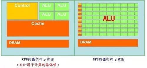
The structure of a CPU mainly includes the Arithmetic Logic Unit (ALU), Control Unit (CU), Registers, Cache, and the buses for data, control, and status communication between them.
In simple terms: computation unit, control unit, and storage unit, structured as shown in the diagram below:
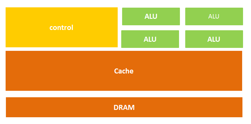
Figure: Schematic of CPU Microarchitecture
What? Can’t remember the architecture? Let’s represent it differently:
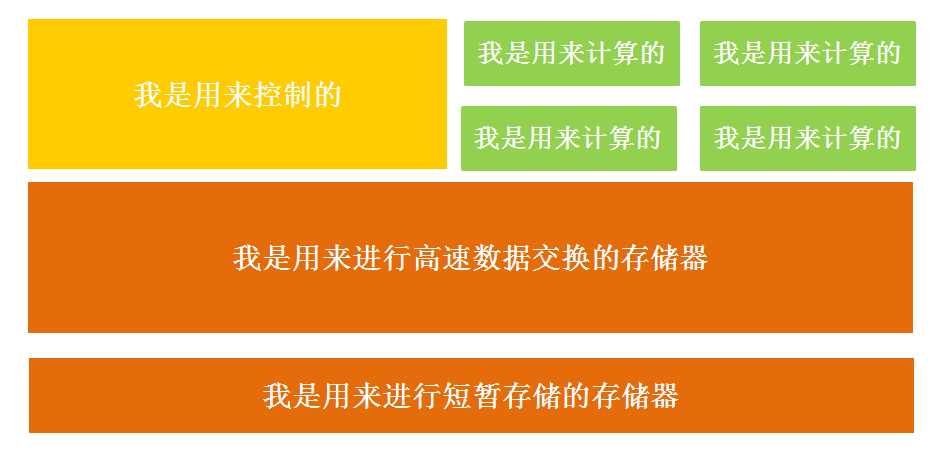
Figure: Schematic of CPU Microarchitecture (Revised)
Yes, that’s roughly the idea.
From the literal meaning, we can also understand well that the computation unit mainly performs arithmetic operations, shifts, and address calculations and conversions; the storage unit is mainly used to store data generated during operations and instructions; the control unit decodes instructions and issues control signals for executing the operations required to complete each instruction.
So the process of executing an instruction in the CPU is as follows: after reading the instruction, it is sent to the controller (yellow area) for decoding via the instruction bus, which then issues the corresponding control signals; then the ALU (green area) performs calculations on the data according to the operation instructions and stores the resulting data in the data cache (large orange area). The process is illustrated in the diagram below:
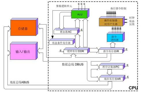
Figure: CPU Instruction Execution Diagram
Is it a bit complex? No worries, you don’t need to memorize this diagram; we just need to know that the CPU follows the Von Neumann architecture, which is fundamentally: store programs and execute sequentially.
At this point, do you see the problem? That’s right— in this structure diagram, the green area responsible for computation seems too small, while the orange area for cache and the yellow area for the control unit occupy a large space.
There is an old saying in high school chemistry: structure determines properties, which is also very applicable here.
Because the CPU architecture requires a lot of space to accommodate the storage unit (orange part) and control unit (yellow part), in contrast, the computation unit (green part) occupies only a small portion, so it is severely limited in large-scale parallel computing capabilities and is better suited for logical control.
Additionally, because it follows the Von Neumann architecture (store programs, execute sequentially), the CPU acts like a meticulous butler, always performing tasks step by step as instructed. However, as the demand for larger scale and faster processing speeds increased, this butler gradually became overwhelmed.
Thus, people wondered if they could place multiple processors on the same chip to work together, thereby improving efficiency. This is how the GPU was born.
GPU
Before formally explaining the GPU, let’s first discuss a concept mentioned earlier—parallel computing.
Parallel computing refers to the process of simultaneously using multiple computing resources to solve computational problems, which is an effective means to improve the speed and processing power of computer systems. The basic idea is to use multiple processors to jointly solve the same problem, that is, to decompose the problem into several parts, each part being computed in parallel by an independent processor.
Parallel computing can be divided into temporal parallelism and spatial parallelism.
Temporal parallelism refers to pipeline technology. For example, in a factory producing food, the process is divided into four steps: cleaning, disinfecting, cutting, and packaging.
If pipeline technology is not used, one food item would complete all four steps before the next one begins, which is time-consuming and inefficient. However, with pipeline technology, four food items can be processed simultaneously. This is temporal parallelism in parallel algorithms, where two or more operations are initiated at the same time, greatly enhancing computational performance.
Figure: Pipeline Schematic
Spatial parallelism refers to multiple processors executing computations concurrently, that is, connecting two or more processors through a network to compute different parts of the same task simultaneously or to solve large problems that a single processor cannot handle.
For example, if Xiao Li plans to plant three trees on Arbor Day, and it takes him 6 hours to complete the task alone, he calls his friends Xiao Hong and Xiao Wang to help on Arbor Day. After 2 hours, each of them completes one tree planting task, which is spatial parallelism in parallel algorithms, where a large task is divided into several identical sub-tasks to speed up problem-solving.
So if the CPU were to execute this tree planting task, it would do it one tree at a time, taking 6 hours, but if the GPU were to plant the trees, it would be like several people planting at the same time.
GPU stands for Graphics Processing Unit, which is a graphics processor. As its name suggests, the GPU was initially used in personal computers, workstations, game consoles, and some mobile devices (such as tablets and smartphones) to perform graphics calculations.
Why is the GPU particularly good at processing image data? This is because each pixel on an image needs processing, and the process and method of processing each pixel are very similar, making it a natural fit for the GPU.
The simple architecture of a GPU is illustrated in the diagram below:
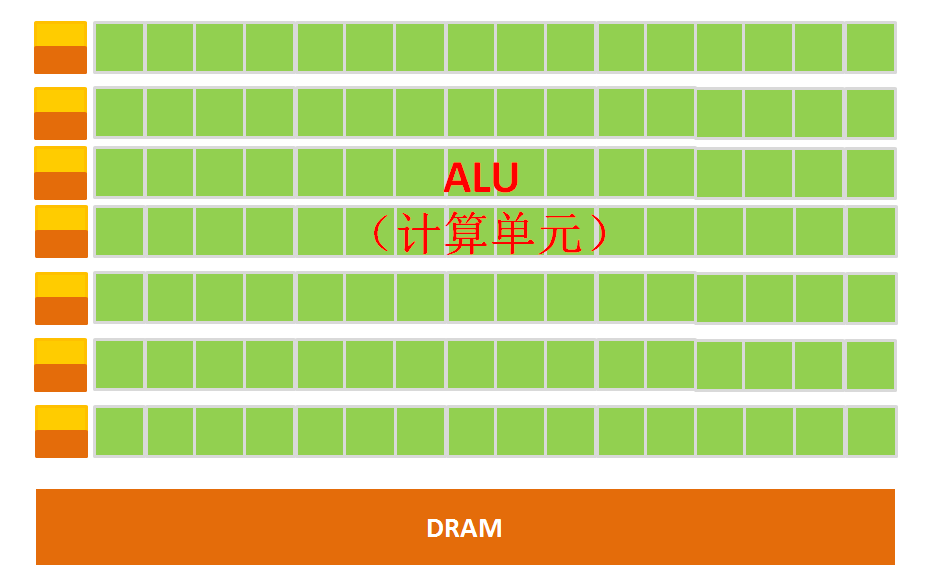
Figure: Schematic of GPU Microarchitecture
From the architecture diagram, we can clearly see that the GPU’s structure is relatively simple, with a large number of computation units and very long pipelines, making it particularly suitable for processing large amounts of uniformly typed data.
However, the GPU cannot work independently; it must be controlled and called by the CPU to function. The CPU can operate independently, handling complex logical operations and different data types, but when a large amount of uniformly typed data needs processing, the GPU can be called for parallel computation.
Note: The GPU has many ALUs and very little cache; the purpose of the cache is not to store data that will be accessed later, which is different from the CPU, but to improve service for threads. If many threads need to access the same data, the cache will merge these accesses and then access the DRAM.
Now, let’s compare the CPU and GPU side by side, and it becomes very clear.
Most of the work done by the GPU involves a large amount of computation but little technical complexity, and it is repeated many times.
To borrow a saying from a certain expert on Zhihu, it’s like you have a job that requires calculating several billion additions and subtractions within a hundred; the best way is to hire dozens of elementary school students to do it, each doing a part, since these calculations are not technically complex, just pure physical labor; while the CPU is like an old professor who can do integrals and differentials, but costs a lot. One old professor is worth twenty elementary school students; if you were Foxconn, who would you hire?
The GPU uses many simple computation units to complete a large number of computational tasks, purely a manpower strategy. This strategy is based on the premise that the work of elementary school student A and elementary school student B is independent of each other.
However, it is important to emphasize that although the GPU was born for image processing, we can see from the previous introduction that it is not structurally designed specifically for image service; it is merely an optimization and adjustment of the CPU’s structure. Therefore, the GPU can not only excel in image processing but is also used in scientific computing, cryptography, numerical analysis, massive data processing (sorting, Map-Reduce, etc.), financial analysis, and other fields that require large-scale parallel computing.
Thus, the GPU can also be considered a relatively general-purpose chip.
TPU
As mentioned earlier, both the CPU and GPU are relatively general-purpose chips, but there is an old saying: the efficiency of a universal tool can never match that of a specialized tool.
As people’s computing needs become more specialized, there is a desire for chips that better meet specific professional needs, leading to the concept of ASIC (Application-Specific Integrated Circuit).
ASIC refers to special specification integrated circuits customized according to product requirements, designed and manufactured according to the needs of specific users and specific electronic systems. Of course, you don’t need to remember this concept; in simple terms, it means customized chips.
Because ASICs are very “specific” and only do one thing, they can perform better than chips like CPUs and GPUs that can do many things in a specific task, achieving higher processing speeds and lower energy consumption. However, correspondingly, the production cost of ASICs is also very high.
The TPU (Tensor Processing Unit) is a chip developed by Google specifically to accelerate deep neural network computation capabilities, which is actually also an ASIC.
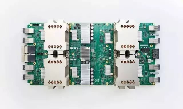
Figure: Google’s Second Generation TPU
Generally, it is difficult for companies to bear the cost and risk of developing dedicated ASIC chips for deep learning, but Google is not just any company; do they lack money?

Just kidding. The more important reason is that many services provided by Google, including Google Image Search, Google Photos, Google Cloud Vision API, Google Translate, etc., require deep neural networks. Given Google’s massive scale, developing a dedicated chip becomes feasible for large-scale applications (spreading the R&D costs across many units).
Thus, it is only natural for the TPU to take the stage in history.
Many machine learning and image processing algorithms used to run on GPUs and FPGAs (field-programmable gate arrays), but these two types of chips are still general-purpose chips, so they cannot closely adapt to machine learning algorithms in terms of performance and power consumption. Google has always believed that great software will shine even brighter with the help of great hardware, so they thought, can we create a dedicated chip for machine learning algorithms? Thus, the TPU was born.
It is said that the TPU can provide a performance improvement of 15-30 times and an efficiency improvement (performance/watt) of 30-80 times compared to contemporaneous CPUs and GPUs. The first generation of TPU could only perform inference and relied on Google Cloud to collect data in real-time and produce results, while the training process required additional resources; the second generation TPU can be used for both training neural networks and inference.
At this point, you might ask, why is the TPU so powerful in terms of performance?
Well, Google has written several papers and blog posts to explain this reason, so I will just touch on it here.
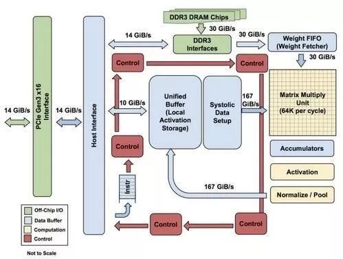
Figure: Block Diagram of TPU Modules
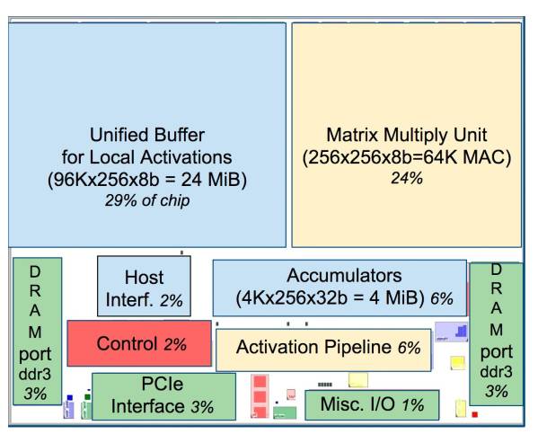
Figure: TPU Chip Layout
As shown in the figure, the TPU uses up to 24MB of local memory, 6MB of accumulator memory, and memory for interfacing with the main control processor, which together occupy 37% of the chip area (the blue part in the figure).
This indicates that Google fully recognizes that off-chip memory access is the main culprit for the low energy efficiency of GPUs, and thus spared no expense in placing a large amount of memory on the chip. In contrast, NVIDIA’s contemporaneous K80 only has 8MB of on-chip memory, requiring constant access to off-chip DRAM.
Additionally, the high performance of the TPU also comes from its tolerance for low computational precision. Research has shown that the accuracy loss from low-precision computation is minimal, but it can bring significant convenience in hardware implementation, including lower power consumption, faster speeds, smaller computation units, and reduced memory bandwidth requirements… The TPU uses 8-bit low-precision computation.
For more information, you can refer to Google’s papers.
So far, the TPU has already accomplished many tasks, such as the machine learning AI system RankBrain, which helps Google process search results and provide users with more relevant search results; Street View, which improves the accuracy of maps and navigation; and of course, the computer program AlphaGo that plays Go!
NPU
At this point, I believe everyone has a certain understanding of these so-called “XPU” technologies, so let’s continue.
The so-called NPU (Neural Network Processing Unit) is a neural network processor. As the name suggests, this chip aims to simulate human neurons and synaptic structures using circuits!
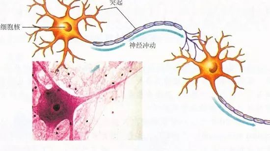
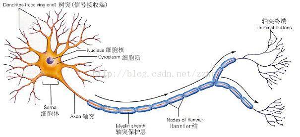
How to imitate? First, we need to look at the human neural structure—biological neural networks consist of several interconnected artificial neuron nodes, with neurons connected pairwise through synapses, which record the connections between neurons.
Do you remember high school biology, comrades?
If we want to use circuits to imitate human neurons, we need to abstract each neuron as an activation function, whose input is determined by the outputs of the connected neurons and the synapses connecting them.
To express specific knowledge, users typically need to adjust the values of the synapses and the topology of the network (through certain specific algorithms). This process is called “learning.”
After learning, the artificial neural network can solve specific problems using the acquired knowledge.
At this point, I wonder if anyone has noticed the problem—originally, since the basic operations of deep learning involve processing neurons and synapses, and traditional processor instruction sets (including x86 and ARM) were developed for general computing, their basic operations are arithmetic operations (addition, subtraction, multiplication, division) and logical operations (AND, OR, NOT), often requiring hundreds or even thousands of instructions to complete the processing of a single neuron, resulting in low efficiency for deep learning processing.
This is when we must take a different approach—break through the classic Von Neumann architecture!
In neural networks, storage and processing are integrated, both represented by synaptic weights. In contrast, in the Von Neumann architecture, storage and processing are separate, implemented by memory and arithmetic units, respectively, leading to significant differences. When using existing classical computers based on the Von Neumann architecture (such as X86 processors and NVIDIA GPUs) to run neural network applications, they inevitably face constraints from the separation of storage and processing, thus affecting efficiency. This is one of the reasons why specialized chips for artificial intelligence have a certain inherent advantage over traditional chips.
Typical representatives of NPUs include China’s Cambricon chip and IBM’s TrueNorth. Taking China’s Cambricon as an example, the DianNaoYu instruction directly addresses the processing of large-scale neurons and synapses, allowing a single instruction to complete the processing of a group of neurons and providing a series of specialized support for the transmission of neuron and synapse data on the chip.
To put it numerically, compared to CPUs and GPUs, NPUs can achieve over a hundred times the performance or energy efficiency ratio difference—based on the DianNao paper published by the Cambricon team in collaboration with Inria—DianNao is a single-core processor with a frequency of 0.98GHz, peak performance reaching 452 billion basic neural network operations per second, with a power consumption of 0.485W at a 65nm process, and an area of 3.02 square millimeters.
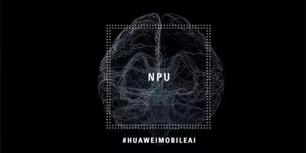
The Kirin 970 chip used in the Mate 10 mentioned at the beginning of the article integrates Cambricon’s NPU, which is why it can achieve the so-called photo optimization function and ensure that your phone remains responsive even after prolonged use (of course, you have to actually use it to know if it lives up to the hype).
PS: The “Star Intelligent No. 1” from Zhongxing Microelectronics claims to be an NPU, but it is actually just a DSP, only supporting forward operations of networks and unable to support neural network training.
With the knowledge above, it becomes easier to understand BPU and DPU.
BPU (Brain Processing Unit) is an embedded AI processor architecture proposed by Horizon Robotics. The first generation is the Gaussian architecture, the second generation is the Bernoulli architecture, and the third generation is the Bayesian architecture. Horizon has already designed the first generation Gaussian architecture and jointly launched the ADAS system (Advanced Driver Assistance System) with Intel at the 2017 CES.
DPU (Deep Learning Processing Unit) was first proposed by the domestic company Deep Vision Technology, based on the reconfigurable characteristics of Xilinx FPGA chips, designing dedicated deep learning processing units (which can design parallel efficient multipliers and logic circuits based on existing logic units, belonging to the IP category), and abstracting customized instruction sets and compilers (instead of using OpenCL), thus achieving rapid development and product iteration. In fact, the DPU proposed by Deep Vision belongs to semi-customized FPGA.
Did you think it was over here?
No, it is said that every 18 days, a new XPU emerges in the integrated circuit field until all 26 letters are used up.
This is humorously referred to as the AI Era’s XPU version of Moore’s Law.
According to incomplete statistics, the following have already been used:
APU — Accelerated Processing Unit, an accelerated image processing chip product launched by AMD.
BPU — Brain Processing Unit, an embedded processor architecture led by Horizon Robotics.
CPU — Central Processing Unit, currently the mainstream product of PC cores.
DPU — Deep Learning Processing Unit, first proposed by Deep Vision Technology; there is also a Dataflow Processing Unit proposed by Wave Computing’s AI architecture; Data Storage Processing Unit, an intelligent solid-state drive processor from Shenzhen Dapu Microelectronics.
FPU — Floating Point Unit, the floating-point operation module in general processors.
GPU — Graphics Processing Unit, designed for graphics processing using a multi-threaded SIMD architecture.
HPU — Holographic Processing Unit, a holographic computing chip and device produced by Microsoft.
IPU — Intelligence Processing Unit, an AI processor product from Graphcore, invested by Deep Mind.
MPU/MCU — Microprocessor/Microcontroller Unit, generally used in low-computation applications of RISC computer architecture products, such as ARM-M series processors.
NPU — Neural Network Processing Unit, a type of processor based on neural network algorithms and acceleration, such as the DianNao series produced by the Institute of Computing Technology, Chinese Academy of Sciences/Cambricon.
RPU — Radio Processing Unit, a processor that integrates Wifi/Bluetooth/FM processing into a single chip, produced by Imagination Technologies.
TPU — Tensor Processing Unit, a dedicated processor launched by Google to accelerate artificial intelligence algorithms. The first generation TPU is aimed at inference, while the second generation is aimed at training.
VPU — Vector Processing Unit, an acceleration core for image processing and AI produced by Movidius, acquired by Intel.
WPU — Wearable Processing Unit, a wearable system-on-chip product launched by Ineda Systems, including GPU/MIPS CPU and other IP.
XPU — An FPGA intelligent cloud accelerator released by Baidu and Xilinx at the 2017 Hot Chips conference, containing 256 cores.
ZPU — Zylin Processing Unit, a 32-bit open-source processor launched by Norway’s Zylin company.
Once all 26 letters are used up, XXPU and XXXPU will soon appear, taking over the naming world at an even faster pace.
Isn’t that scary?
At this point, I believe everyone has a preliminary understanding of these XPU concepts.
But do you think that after explaining all this to the ladies, you will successfully win their hearts?
Too naive!
The essence of the questions ladies ask is just one: Stop babbling, go order it for me!
That’s all, have a great weekend~
The IoT Think Tank has specially launched the “Beginner’s Series” column to popularize seemingly complex and profound technological concepts.
If you have any content you want to see, feel free to leave a message in the comment section!

Previous Popular Articles (Click the title to read directly):
-
“How Difficult Is It to Make an Intelligent Lock for Shared Bicycles?”
-
“A Cartoon Explains: Besides WiFi and Bluetooth, What Can the Recently Popular NB-IoT Do?”
-
“A Cartoon Explains: Behind NB-IoT, What Is LoRa That Everyone Is Talking About?”