As the demand for faster and cheaper non-volatile memory alternatives continues to grow, especially in applications such as automotive, resistive RAM (ReRAM) is back in the spotlight.
Embedded flash has long left designers hoping for better write speeds and lower power consumption, but as the leading edge of this technology shrinks to 28nm, another issue arises. Manufacturing flash at these dimensions may require a dozen masks, which increases costs. Additionally, flash requires high power consumption and relatively high voltage at the front end.
This is precisely where potential competitors see an opportunity, as they try to adopt ReRAM. A key argument from ReRAM supporters is that some new applications demand higher performance, which cannot be achieved simply by scaling up flash.
In a deeply entrenched memory market, it is often difficult for newcomers and new technologies to break in, partly because it is hard to compete on cost with chip manufacturers whose fabs and equipment have largely been depreciated, and partly because existing technologies have proven to work well over time. Moreover, in a market with multiple players, relevant companies are continuously innovating to stay competitive. Therefore, if these other technologies can establish themselves, they are likely to find a place in the high-end NOR flash market, where there are new opportunities and higher product prices, rather than in the mainstream market where NOR flash may still be viable.
This is especially true in many automotive applications, where cost is a key factor. “A typical car has about 20 flash memories,” said Jackson Huang, Vice President of Marketing at Winbond Electronics. “Six to eight cameras in a car have flash. The dashboard also uses flash, and the infotainment system uses flash as well. The MCU has a certain amount of flash built in. But what really drives this market is the significant increase in flash usage in the past few years, both in terms of density and unit shipments, due to the emergence of OTA (over-the-air) images.
Xi-Wei Lin, Director of Application Engineering at Synopsys EDA Group, also believes that there will be multiple options in the future. “ReRAM can be used as embedded memory for IoT devices, and it can also serve as a standalone unit within MCUs,” he said. “ReRAM is not susceptible to magnetic attacks, which makes it potentially useful for applications in special environments or for unique security needs. NVM will continue to be the choice for specific applications, depending on performance, power, reliability, density, form factors, and cost. There are always trade-offs; in my opinion, there is no one-size-fits-all solution.”
Market research also supports these conclusions. According to Business Market Insights, the NOR flash market is growing at a compound annual growth rate (CAGR) of 14%, expected to reach $1.64 billion by 2028. Meanwhile, according to Data Bridge Market Research, the value of ReRAM is expected to surpass NOR flash in the coming years, with a CAGR of 17.2%, projected to reach $2.16 billion by 2030. Companies remain optimistic about all these memory chips, especially considering heterogeneous integration and the rapidly growing volume of data.
Jack Guedj, CEO of Numen, stated, “Next-generation persistent memory has many advantages over traditional NOR flash, but they suffer from low endurance and poor write performance.” He added, “For some applications, the read performance is also too slow, and the active read power is too high. This means SoC designers either read/write directly from these memories or add a large SRAM buffer to the ReRAM, thereby avoiding heavy penalties in performance and power.”
ReRAM has been hit hard by HP’s abandonment, but it has matured in recent years. Existing memory companies and some startups have researched the tricky materials science needed to achieve consistent results. In academic and corporate research labs, ReRAM has become the preferred memory for neuromorphic artificial intelligence applications, as demonstrated by the NeuRRAM chip created last year by academic partners from the University of California San Diego and Stanford University.
Tony Kenyon, Professor at University College London and CTO of ReRAM startup Intrinsic, reflected on the efforts to solve fundamental challenges such as stability. “As far back as seven or eight years ago, many papers were published, with research groups either studying the periodic table of oxide elements or doping different elements into oxides, trying some devices, and then moving on to the next device.”
In one such effort, IBM chose HfO2-based ReRAM because it was already familiar with this material from its pioneering work on hafnium in logic transistors. IBM is now tuning it to meet the demands of deep learning.
Intrinsic chose to use silica. “We can do some more interesting things with oxides,” Kenyon explained. “We can use a nominally very insulating material, a very good dielectric, and by constructing the oxide in a specific way, rather than making a very defect-free uniform, flat interface stoichiometric oxide that has been used for decades, we can design it in a slightly different way to make it switchable states, high resistance state and low resistance state. Depending on how we program and create the device, it could even have more states, in some sense, even simulating resistance changes, but for memory devices, for ReRAM memory devices, two states are a good starting point.”
Potential eFlash Alternative
ReRAM is now one of the main competitors to replace high-end embedded flash (eFlash), although it is unlikely to replace NAND flash. As noted in Objective Analysis’s 2023 Emerging Memory Report, “Over time, NOR flash embedded in most SoCs will be nearly completely replaced by MRAM, ReRAM, FRAM, or PCM, which will also help drive the success of independent new memory chips.”
Gary Bronner, Senior Vice President at Rambus Labs, stated, “Compared to embedded flash, ReRAM requires fewer masks for integration with CMOS processes, can scale to smaller nodes, and is byte-addressable. The main metric for traditional NAND flash is bit cost, where ReRAM is not competitive.”
Another example of ReRAM gaining traction is that Weebit Nano’s ReRAM is now fully qualified for use with SkyWater Technology’s 130nm CMOS process.
Additionally, TSMC and Infineon have been collaborating for years to develop ReRAM (also known as RRAM), now incorporating it into automotive microcontrollers.
Sandeep Krishnegowda, Vice President of Marketing and Applications at Infineon, stated, “A few years ago, as we moved toward advanced process nodes, we decided that RRAM was the right choice for embedded memory.” He added, “It is a low-power technology. It is byte-addressable, so unlike flash, you can write directly. Endurance and retention performance are comparable to flash, and it is cheaper. We have been developing the technology and algorithms for RRAM in collaboration with TSMC for over a decade. Initially, we used RRAM in some chip cards that could be used for cashless payments and secure identification. In the consumer industrial market for controllers and MCUs, we use this memory as an alternative to embedded flash. Recently, we have introduced it into the automotive sector.”
For chip cards, another advantage of ReRAM is its high resistance to electromagnetic interference. Krishnegowda noted, “If you think about payment cards and how everyone wants to extract information, you would want your memory to be very robust.”
Moreover, ReRAM does not have leakage issues, according to Kenyon.
Basics of ReRAM
The materials science behind ReRAM is extremely complex, but the basic theory is relatively simple. ReRAM uses resistance as the basis for switching rather than charge.
Mark Dickinson, CEO of Intrinsic, explained, “Basically, it is a resistor with variable resistance that can be changed by applying a specific voltage, and it can be reset.”
At the core of ReRAM operation are conductive filaments that form and break by two different methods. In OxRAM, a metal oxide material is sandwiched between two electrodes. When a positive voltage is applied to the top electrode, conductive filaments form between the two electrodes. The filaments are composed of oxygen vacancies. When a negative voltage is applied to the bottom electrode, the conductive filaments break. Essentially, ReRAM switches between high resistance state and low resistance state. The change in resistance is represented by “0” and “1” in memory.
However, in CBRAM, copper or silver metal is injected into silicon to form conductive bridges or filaments between the two electrodes.
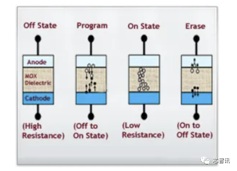
Figure 1: How ReRAM Works. Source: Adesto Technologies
Most commercial work, such as the collaboration between TSMC and Infineon, now focuses on OxRAM.
Ilan Sever, Vice President of R&D at Weebit Nano, stated, “Both are called resistive RAM because both involve changing the resistance of certain storage elements, but they are quite different in terms of physics and chemistry.” He added, “In oxygen vacancies, we apply different voltages across the resistance layer and then generate or dissolve conductive filaments based on the applied voltage. This way, we can reset the battery—that is, we dissolve the filaments so that they no longer conduct, resulting in high resistance. We call this the zero state or reset.”
Kenyon from Intrinsic further explained, “We are changing something in the oxide, and we are creating a filament that connects the gap between the two electrodes. These devices are very simple capacitive structures with just one layer of oxide and an electrode on top. We can create a conductive filament that connects the two batteries. This filament is composed of oxygen vacancies. So we are actually moving some oxygen.” We form filaments in the oxide and then move from the original, truly high resistance state to the low resistance state. When we reverse polarity, we move the oxygen back in the other direction and re-oxidize a small part of the filament, not all of it, and then we can move back and forth many times between low resistance and high resistance states.”
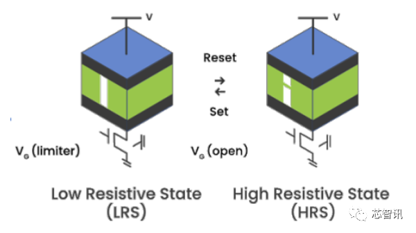
Figure 2: ReRAM Resistance. Source: Weebit Nano
Drawbacks of ReRAM
Like all memory technologies, ReRAM has its vulnerabilities.
Takashi Ando, Chief Research Scientist at IBM, stated, “The fundamental challenge ReRAM faces is that it is noisier than other material options.” He explained, “In oxide ReRAM, we move oxygen vacancies randomly. In CBRAM, cations are used in a random manner. There is some randomness in the operation of the device, which is accompanied by high noise, so the inherent noise level is the biggest challenge, but it is more robust against external stimuli compared to MRAM or other memories.”
The impact of this noise should not be underestimated. Lin from Synopsys stated, “The biggest problem with ReRAM is its inherent variability (noise) at the single cell level.” He noted, “The change in resistance from one switching cycle to another can be as large as the change in resistance across a population of cells. For filament-based ReRAM, such as OxRAM and CBRAM, the resistance values are controlled by a small number of oxygen vacancies or metal atoms moving around the filament tip at high electric fields and/or high local temperatures. This process is essentially random; a few atoms or vacancies can produce significant variations. So noise is inherent. Increasing the switching current can mitigate variability to some extent, but at the cost of power consumption.”
Kenyon downplayed this impact. He said, “The traditional industry view is that ReRAM has a variability problem because it is inherent in the process of making these filaments, and there is nothing you can do about it. But it actually comes down to material engineering issues. We have demonstrated that by designing materials the right way, we can reduce the variability of programming voltages, for example, the distribution of different voltages required to switch from high resistance state to low resistance state.”
Takeo Tomine, Product Manager for Ansys’s Totem, also pointed out that heat is a problem for ReRAM. “Typically, for advanced technology nodes below 7nm, when the power supply voltage (Vdd) has been constant—leading to higher power densities and greater metal densities, resulting in more heat. The self-heating effect is a key factor affecting ReRAM reliability and accuracy. When heat is trapped in transistor devices, self-heating becomes most severe. For ReRAM, temperature variations reduce the Ron/Roff ratio, which negatively impacts the accuracy and reliability of many applications, including AI processing. Careful thermal management is a must, especially in designs where power consumption is uneven across different devices. Then, the heat generated must be modeled for its propagation to nearby layers and devices to capture the heat changes over time across the entire chip.”
Xi-Wei Lin added, “A major challenge ReRAM technology faces is the lack of quantitative physical models for multi-physics (i.e., electro-thermal-chemical issues). Empirical models do exist, but there is a lack of fundamental physics. Without good models, it is difficult to control or optimize the manufacturing process.”
Conclusion
ReRAM’s competitors will not back down without a fight. Guedj from Numen stated, “ReRAM-type technologies have relatively slow write times, around 20,000 to 30,000 nanoseconds. SRAM is about 1 or 2 nanoseconds.” He claimed that Numen’s latest technology can reduce ReRAM write times by a factor of 100, or that Numen’s MRAM can further reduce it to around 50 nanoseconds, although the challenge for MRAM is higher processing costs. “More technological advancements are needed. Flash cannot shrink further. For MRAM, the challenge is to lower processing costs, which may happen over time. Most major foundries will keep their options open, with both sides trying and hedging bets.”
Others believe ReRAM will win. Jongsin Yun, memory technology expert at Siemens EDA, stated, “ReRAM offers two major advantages over MRAM—simpler processes and a wider read window.” He explained, “MRAM requires more than 10 layers of stacking, all of which need to be controlled very precisely to form matching crystalline structures. This is a challenge for maintaining high yield. In contrast, the stacking of ReRAM is much simpler, requiring relatively less effort to maintain yield. Additionally, MRAM’s read window is very narrow (on/off ratio), making it very susceptible to failure due to small resistance shifts. On the other hand, ReRAM has a higher-order read window, making it less susceptible to parasitic resistance shifts.”
However, in a critical area, MRAM is ahead, making ReRAM less likely to be a suitable choice for last-level cache. Jongsin Yun stated, “The typical speed of ReRAM is on the order of microseconds to hundreds of nanoseconds, making it unsuitable for use as last-level cache (LLC). As for endurance, ReRAM products typically have endurance around 1E5 (100,000 write cycles), far below the requirements for LLC (1E12 cycles). Due to these limitations, there is much more discussion about MRAM for last-level cache. Adesto was later acquired by Dialog Semiconductor (which was subsequently acquired by Renesas), demonstrating ReRAM write speeds of up to 10ns. In contrast, a joint team from IBM and Samsung demonstrated MRAM Mbits at 250ps, indicating a significant speed difference.”
For this and other reasons, NVM is likely to have multiple options in the foreseeable future.
Ando from IBM stated, “It is more natural to let NVM suitable for each application become the standard rather than dreaming of a one-size-fits-all memory.” He added, “My expectation is that we will see customized NVM for each application, which is already in the works for inference and training.”
Finally, Bronner from Rambus stated that both MRAM and ReRAM as embedded memory seem to be gaining popularity. “Overall, MRAM’s performance seems to be slightly higher, but its cost is also higher. ReRAM is cheaper but may not reach the same level of performance and reliability. Everyone should be able to find a home, depending on the trade-offs their end customers are willing to make.”
Compiled by: Chip Intelligence – Lin Zi Source: semiengineering.com
247 billion acquisition of H3C transaction “terminated”! Unisplendour shares plummet nearly 7%!
Huawei’s autumn full-scene product launch: Honghu 900, Kirin A2, Star Flash technology unveiled!
41 signed projects, investing 32.42 billion yuan! Huangshi optoelectronic information industry is rising strongly!
Qualcomm’s massive layoffs in China? It is rumored that the WiFi department will be cut entirely, and other departments may cut 20%, with compensation of N+7!
Weilai self-developed laser radar master control chip released: 8-core CPU, mass production in October!
Intel fully powers AI! Gaudi3, Core Ultra, 288-core Xeon exposed!
Ren Zhengfei’s latest speech: Don’t be exclusive, Apple is Huawei’s “teacher”!
Replacing traditional packaging substrates, Intel’s “glass core substrate” technology exposed!
Photolithography machine factory? No! This is Beijing’s high-energy synchrotron radiation source!
1.5 Exaflops! China’s new generation supercomputer exposed!
Stock price soared by 25%, Arm’s market value approaches 480 billion yuan! Facing the challenge of RISC-V, can profit margins reach 60%?