
Grounding is crucial when designing printed circuit boards (PCBs). One common method is star grounding. But what exactly is star grounding? And why is it important for your PCB design? Let’s break it down.
What is Star Grounding?
Star grounding is a method of connecting different parts of a circuit to a single grounding point. Imagine a star. The center is the ground, and all parts of the circuit connect directly to the ground, like the points of a star. This method helps maintain the same ground potential across the entire circuit board.
Star grounding ensures that all parts of the circuit “see” the same ground. This helps prevent unnecessary noise and interference. It’s like everyone in a room listening to the same person speak, without any echoes or distractions.
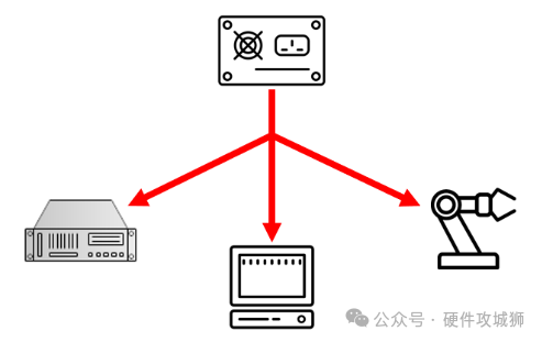
The Importance of Proper Grounding in PCB Design

Proper grounding is key to PCB design. With it, your circuit can avoid serious issues. Grounding keeps signals clean and components safe. It’s like the foundation of a building; if the foundation is weak, the entire structure is at risk.
Learn more about understanding electronic components: the cornerstone of modern technology.
Star grounding is a method to ensure proper grounding. Connecting all grounds to a single point can reduce the likelihood of noise and interference.
This is especially important for circuits handling both analog and digital signals. These different types of signals can easily interfere with each other, leading to circuit failures.
In short, good grounding practices (like star grounding) are essential for reliable and efficient PCBs. They help ensure your circuit works as intended without unexpected issues.
How Star Grounding Works

Star grounding may sound complex, but it becomes easier to understand once broken down. Let’s delve into the basics and its importance in PCB design.
The Basic Principles of Star Grounding

The core idea of star grounding is simple. You connect different parts of the circuit to a single grounding point. Imagine a star. The center of the star is your main ground. The lines extending out are the connections to the various parts of the circuit.
Each part of the circuit has a direct path to the central ground. This setup helps prevent noise from propagating between different parts, keeping signals clean and reducing interference.
Why is this important? Different parts of a complex circuit can generate noise. Without proper grounding, this noise can propagate and cause problems. Star grounding prevents this by connecting each part directly to the ground.
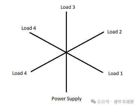 Star Grounding Topology
When we talk about star grounding topology, we refer to how everything is laid out. In this setup, the ground connections form a star shape. The central grounding point is like the hub of a wheel, and the parts of the circuit are like the spokes.
This layout is crucial because it minimizes the possibility of ground loops. Ground loops can introduce unnecessary noise and even damage your components. By connecting everything to a single point, you can avoid these issues.
It’s worth noting that star grounding works best in certain situations. For example, it is very effective in mixed-signal circuits where analog and digital signals coexist. These signals can interfere with each other, but star grounding helps keep them separate.
However, there are better options than star grounding. In some cases, a continuous ground plane may be better for high-speed digital circuits. But for many PCB designs, especially those with mixed signals, star grounding provides a simple and effective solution.
Applications of Star Grounding in Mixed-Signal PCB Design
Star grounding is not just a fancy term; it is a practical concept with real applications, especially in mixed-signal PCB design.
Let’s explore its common scenarios and reasons.
Star Grounding in Analog and Digital Circuits

In mixed-signal PCBs, there are often both analog and digital circuits present at the same time. These two types of circuits don’t mix well, like oil and water.
Get a detailed guide for designing PCBs for mixed-signal systems..
Analog circuits handle continuous signals, while digital circuits deal with 1s and 0s. The problem? Digital circuits generate noise that disrupts the smooth flow of analog signals.
This is where star grounding comes into play. Each part of the circuit has its direct grounding path, minimizing interference.
Think of it like having separate lanes on a highway. Each car (or signal) stays in its lane, reducing the chances of collisions (or interference). This setup is crucial for circuits where precision and noise reduction are paramount.
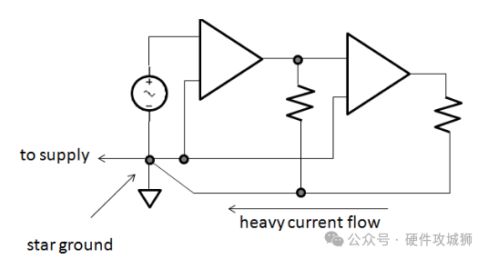 Why Star Grounding is Common in Audio Circuits
Audio circuits are susceptible to noise. Even a small amount of interference can lead to unwanted hum, buzz, or distortion. That’s why star grounding is often used in audio circuits.
Audio circuits may have multiple parts: power supply, signal processing, and output stage. Without proper grounding, each part can introduce noise.
Star grounding helps connect each part directly to the central grounding point. This can prevent noise from spreading to another part.
For example, the power supply may generate some noise. If this noise enters the signal processing part, it can degrade audio quality. But with star grounding, the noise is contained within the power supply section, keeping the audio signal clean and clear.
This is why star grounding is so common in high-fidelity audio devices. It ensures that the sound you hear is pure, without unnecessary interference. In short, star grounding helps maintain the integrity of audio signals, providing a better listening experience.
Challenges of Implementing Star Grounding
While star grounding has its benefits, it also comes with challenges. In modern PCB design, these challenges can be quite severe. Let’s look at why implementing star grounding can be difficult.
The Complexity of Modern PCB Design
Modern PCBs are more complex than ever. They often have multiple layers, a large number of components, and high-speed signals. This complexity makes it difficult to effectively implement star grounding.
In simple circuits, connecting everything to a single grounding point is straightforward. But in complex PCBs, this can become a logistical nightmare.
Routing all ground connections to a central point can lead to long traces, increasing resistance and inductance. These can cause delays and lead to signal integrity issues.
Ensuring that all ground connections lead to a single point on every layer of a multilayer PCB is a challenge. It requires careful planning and precise execution. If not handled properly, it can lead to poor performance and increased noise.
Therefore, while star grounding sounds simple in theory, putting it into practice in modern designs is anything but.
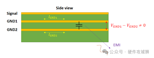 The Risk of Electromagnetic Interference (EMI)
Electromagnetic interference (EMI) is a major concern in PCB design. If implemented incorrectly, star grounding can increase the risk of EMI.
One of the main issues is the potential for large loop areas. Long-distance signals reaching the central grounding point can create large loops.
These loops can act like antennas, picking up and radiating EMI. This defeats the purpose of star grounding, which is to reduce noise.
Another area of concern is the gaps between different ground regions. If a signal crosses this gap, it can create a high-impedance path. This path can generate EMI, leading to circuit problems.
In summary, while star grounding aims to reduce noise, improper implementation can lead to more EMI rather than less. Careful consideration of layout and routing is crucial to avoid these pitfalls.
Learn more about the causes and solutions for electromagnetic interference (EMI) in PCB design..
When Should You Use Star Grounding?
Star grounding is not always the best choice, but sometimes it shines. Let’s discuss when star grounding is truly beneficial.
Specific Situations Where Star Grounding is Beneficial
Star grounding works well in specific situations. One of them is in circuits where noise is a major concern. If your design has sensitive analog signals, star grounding can help keep those signals clean. It can prevent noise from the digital parts from entering your analog path.
Another situation is in audio circuits. Here, even small amounts of noise can ruin sound quality. Star grounding can prevent this by isolating audio signals from potential sources of interference.
Consider star grounding in low-frequency circuits. In these designs, signals move slowly, so the risk of long grounding paths is lower, making star grounding a practical choice.
Examples of Effective Star Grounding Implementation
Let’s look at some examples of effective star grounding.
First, star grounding is often the preferred method for high-end audio equipment. These devices require pristine sound quality, free from hum or buzz.
By connecting all different parts of the circuit to a single grounding point, designers can minimize interference and ensure the sound remains clear.
Another example is precision measurement devices. These devices need to detect the smallest changes in signals.
Any noise can lead to incorrect readings. Star grounding helps isolate sensitive parts of the circuit, ensuring that noise from other parts does not affect measurements.
Finally, star grounding is helpful for simple low-frequency circuits (like circuits in basic analog designs).
These circuits do not need to handle high-speed signals, so there’s no need to worry about the potential issues of long grounding paths. Star grounding helps maintain signal integrity without the complexity of more advanced grounding methods.
Best Practices for Star Grounding in PCB Design

Implementing star grounding correctly requires some expertise. Let’s explore the best ways to achieve it in PCB design.
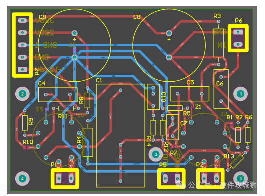
How to Implement Star Grounding Correctly

First, carefully plan your layout. Before placing any components, decide where your central ground point will be. This point is crucial because all ground connections will lead to it. Think of it as the heart of the circuit.
Learn more about how to design PCB layouts?
Next, keep the connections short. The shorter the path to the central ground, the better. Long paths introduce resistance and inductance, leading to noise and signal delay issues. Try to arrange your components to minimize the distance to the central ground.
Another key point is to separate the analog and digital grounds until they meet at the central point. This separation can prevent digital noise from interfering with analog signals. It’s like having a noisy party in one room while a quiet study session takes place in another room.
Finally, avoid routing signals over gaps in the ground plane. This can create loops that act like antennas, picking up unwanted noise. Instead, ensure that each signal has a direct path to the central ground.
Tools and Techniques for Optimizing PCB Grounding
Using the right tools can make star grounding easier and more effective. PCB design software often includes features that assist with grounding. For example, you can use these tools to visualize your ground paths and ensure they are as short and direct as possible.
Simulation tools are also valuable. They allow you to model your design before building the PCB. You can test different grounding strategies and see how they affect performance. By identifying potential issues early, you can save time and money.
Another tip is to use ground planes wisely. While star grounding relies on a central point, combining it with a continuous ground plane can provide additional stability. This hybrid approach can give you the best of both worlds, especially in complex designs.
Additionally, consider using decoupling capacitors. These components help filter out noise, making grounding more effective. Place them near power connections to eliminate any fluctuations.
Finally, be sure to double-check your design. Before finalizing, review your layout for potential issues, such as long ground paths or poorly placed components. Careful checking can catch small errors that could lead to big problems later.
Conclusion
Star grounding is sometimes the preferred solution in today’s PCB design. It is particularly suitable for specific scenarios, such as low-frequency analog circuits or high-fidelity audio designs.
However, other grounding methods may be more effective for many modern applications, especially those involving high-speed signals. The key is to understand the needs of the circuit and choose the grounding strategy that best fits those needs.
If you decide to use star grounding, plan carefully. Ensure your layout is clean and connections are short. Use the right tools and techniques to avoid common pitfalls. If done correctly, star grounding can provide significant benefits.
END


Some screenshots of electronic books

【Complete Collection of Hardware Learning Materials】