The mechanical dimensions and surface conductors of printed circuit boards directly reflect the CNC processing and wet process capabilities of the PCB production line. This is a mandatory inspection item for finished PCBs, commonly used testing instruments include Automatic Optical Inspection (AOI) and Coordinate Measuring Machines (CMM).
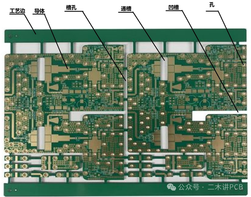
Figure 1 Mechanical dimensions and conductors of PCBs
Mechanical Dimensions:
1) Edge (Periphery)
The non-functional area around the PCB, usually referred to as the “process edge”, is mainly used for clamping and fixing by equipment. After assembly, this part will be removed, and the dimensional tolerance is generally required to be -0.2~0mm.
2) Thickness (Thickness)
The Z-direction dimension of the PCB, with a dimensional tolerance generally required to be ±10%.
3) Cutout (Cutout)
To achieve functions such as weight reduction, mechanical positioning, and electromagnetic shielding, some hollow cavities are evenly distributed inside the printed board, with a dimensional tolerance generally required to be 0~+0.1mm.
4) Slot (Slot)
Slots can achieve functions such as multi-piece assembly, mechanical installation, and electrical isolation, with a dimensional tolerance generally required to be 0~+0.1mm.
5) Notch (Notch)
Part of the PCB’s outline, it can achieve mechanical adaptation and installation positioning, with a dimensional tolerance generally required to be 0~+0.1mm.
6) Hole (Hole)
To achieve three-dimensional electrical interconnection, mechanical positioning, and electromagnetic shielding, the PCB contains a large number of blind holes, buried holes, through holes, back-drilled holes, and non-support holes, with hole diameter, position accuracy, hole spacing, and hole ring all needing to meet the corresponding standards for product grade requirements.
7) V-type Scoring (Scoring)
Commonly known as V-Cut, it is achieved by using a V-shaped milling cutter (with blade angles typically of 30°, 45°, 60°) to cut a recess at designated positions on the PCB assembly, leaving a remaining thickness of 0.3~0.8mm. The PCB substrate at the V-cut is weakened, becoming a “stress concentration point”, and when separating the board, only a slight vertical force is needed, and the PCB will break precisely along the V-cut’s “V” shape.
8) Edge printed board contacts to connector key area (edge printed board contacts to connector key area)
Commonly referred to as the “gold finger” position, it is the key interface for the PCB to transmit electrical signals between external devices, other circuit boards, or interfaces. When the connector is inserted, its internal metal contacts will precisely contact these contacts on the edge of the PCB, achieving electrical conduction.
9) Warpage (Warpage) and Twisting (Twisting)
Caused by uneven wiring of the PCB, asymmetric stacking structure, and large aspect ratio, the board surface may experience “upward and downward bulging / concave planar deformation” (warpage) or “diagonal lifting three-dimensional deformation” (twisting), affecting component soldering, overall assembly, and circuit reliability, generally required to be <0.75%.
Conductors (Wires, Pads, and Power/Ground Planes)
1) Conductor Width and Thickness (Conductor Width and Thickness)
Domestic and international standards have lower requirements for the width and thickness of conductors on ordinary digital boards, but for some special applications, personalized specifications need to be determined. For example, conductor width is a key indicator that determines characteristic impedance, directly affecting the integrity of high-frequency and high-speed signals. Therefore, for such products, the precision of conductor width is not explicitly specified, but the range of characteristic impedance is generally required to be ±5%.
2) Conductor Spacing (Conductor Spacing)
Close proximity between two conductors can create parasitic capacitance, potentially leading to signal crosstalk or high-voltage breakdown risks, as high-frequency / high-speed circuits and high-voltage power supplies have strict requirements for conductor spacing.
3) Conductor Imperfections (Conductor Imperfections)
Conductor cross-sectional area or surface area reduction due to pinholes, scratches, serrations, dents, cracks, etc., can affect electrical continuity.