01 Industry Chain Overview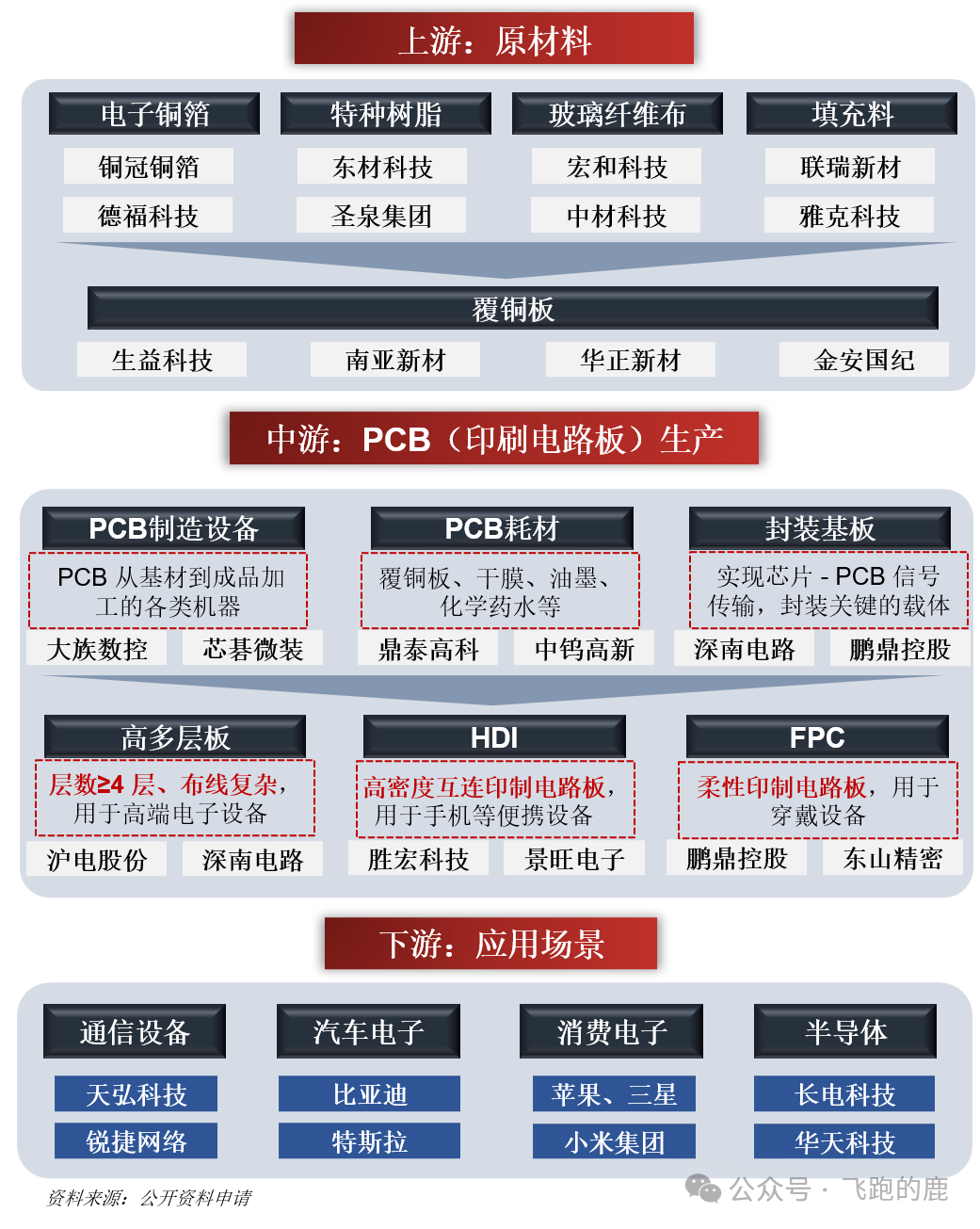 02 Introduction to PCB
PCB stands for Printed Circuit Board, also known as a printed wiring board. It serves as the “connection hub + support frame” for electronic products—its core function is to connect various electronic components through circuits, allowing for smooth transmission of current and signals, acting as a crucial “connecting bridge”.Almost all electronic devices rely on it: it not only provides support as a “mounting base” for electronic components but also plans the circuitry, enabling power supply or insulation, ensuring electrical performance.
The quality of PCB manufacturing directly affects the stability and longevity of electronic products, and it also influences the overall competitiveness of the product, which is why it is referred to as the “mother of electronic products”.
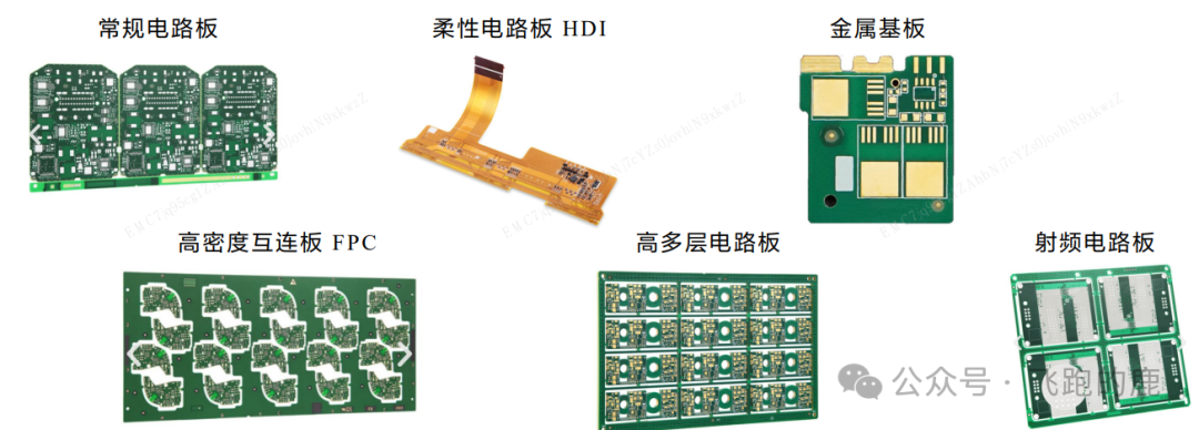
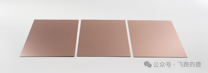
PCB Diagram
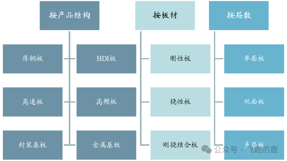
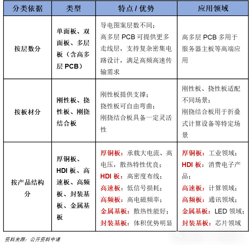
There are many classification methods for PCBs, but the three commonly used in the industry are: one based on the number of conductive layers, one based on the material of the board, and one based on the structure of the product itself.
03 Market Size
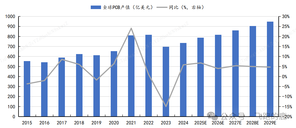
With market inventory adjustments and a softening demand for consumer electronics coming to an end, coupled with accelerated AI applications, the reduction in inventory and interest rate hikes in 2023 have passed, and the PCB industry is entering a new growth cycle.
In 2024, the global PCB market value is projected to reach $73.565 billion (up 5.8% year-on-year), and it is expected to reach $94.661 billion by 2029, with a CAGR of 5.2% from 2024 to 2029, indicating a revival in global market value.
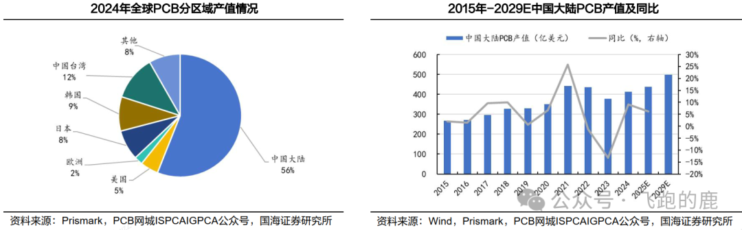
Since 2006, mainland China has surpassed Japan to become the world’s largest PCB production base, marking a shift in the industry landscape; in 2024, the mainland’s output value is expected to reach $41.213 billion, accounting for 56% of the global total (Prismark data).
Global PCB production capacity is shifting to the mainland, driven by the development of downstream electronic terminal industries, consumer electronics, AI, and new energy vehicle applications, which are boosting PCB demand. Prismark predicts that by 2025, the mainland’s output value will reach $43.734 billion (up 6.1% year-on-year), and by 2029, it will reach $49.704 billion, with a CAGR of 3.3% from 2025 to 2029.
 04 Cost Breakdown
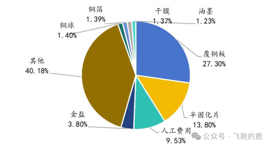
According to relevant data, the cost breakdown of PCBs is as follows, with copper-clad laminates holding the highest cost:
Scan below to join directly:

05 Copper Clad Laminate
Copper Clad Laminate (CCL) is the core material for making PCBs, akin to the “load-bearing wall of a house”—first, electronic fiberglass cloth and other reinforcing materials are soaked in resin adhesive, dried, cut into blanks, and then copper foil is hot-pressed onto one or both sides to form a shape, ultimately enabling the PCB to achieve interconnection of components, isolation of current, and structural support.
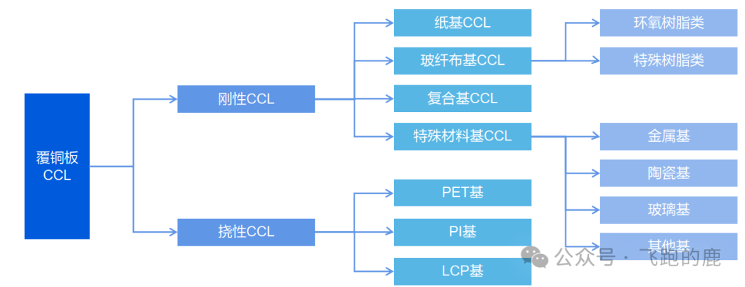
Based on composition materials and mechanical properties, common copper clad laminates are mainly divided into two categories: “rigid” and “flexible”. Rigid CCLs are further divided into paper-based, fiberglass cloth-based, composite-based, and special material-based; flexible CCLs are categorized into PET-based, PI-based, and LCP-based.
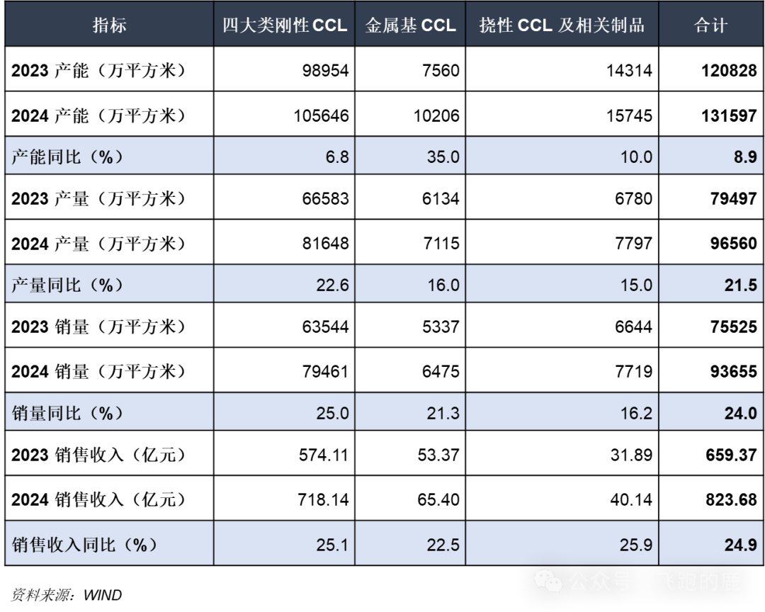
In 2024, both the production and sales of copper clad laminates in China are expected to achieve rapid growth, as detailed below:
05-1, Copper Foil
PCB copper foil is a thin layer of copper deposited on the substrate of the circuit board, equivalent to the “signal transmission line” of the circuit board, and is an important raw material for manufacturing CCL and PCB, with the core function of signal transmission. It is made together with electronic-grade fiberglass cloth, special wood pulp paper, synthetic resin, and other materials to form copper clad laminate, which is then processed through a series of processes to ultimately form the PCB.
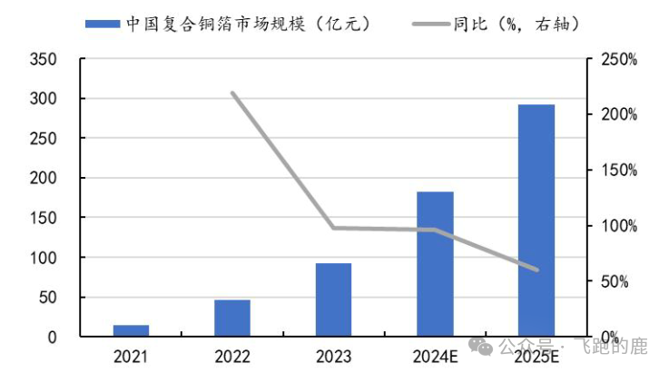
Currently, domestic composite copper foil has entered a critical stage of material certification and loading tests, and is expected to achieve a breakthrough from 0 to 1 in large-scale applications. The market forecast changes are as follows:
05-2, High-Frequency High-Speed Copper Clad Laminate
High-speed copper clad laminate is like a “high-speed network cable” in the circuit board, capable of achieving fast signal transmission of 10-50Gbps, with high accuracy, minimal signal dispersion, and low loss, primarily used in data processing centers, servers, switches, and routers.
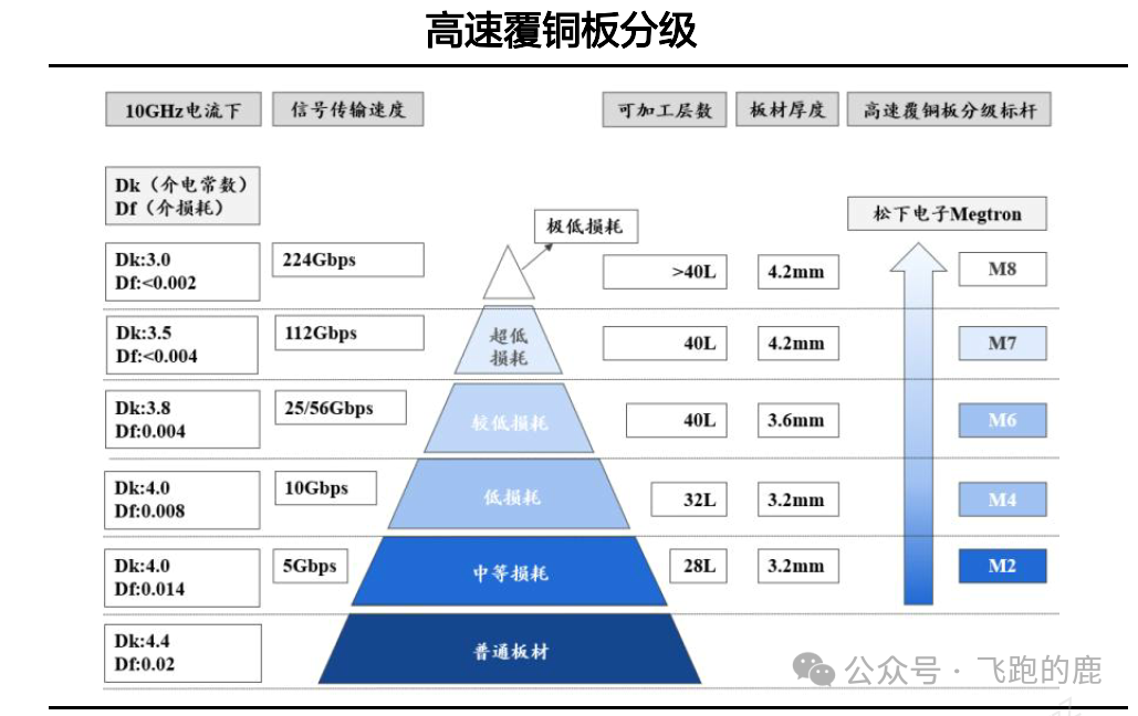
High-frequency copper clad laminate (High Frequency Copper Clad Laminate) is a “dedicated receiver” for ultra-high frequency signals, operating at frequencies above 5GHz, suitable for ultra-high frequency scenarios, requiring ultra-low dielectric constant (Dk) and as low as possible dielectric loss (Df). It is a core material for 5G base stations, autonomous driving millimeter-wave radar, and high-precision satellite navigation, with demand continuously increasing.
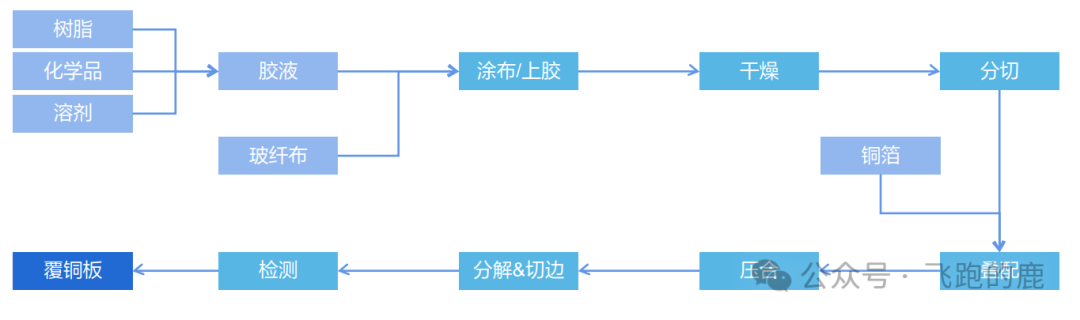
Like high-speed copper clad laminates, to reduce Dk, it mainly relies on modifying insulating resins, fiberglass, and overall structure. Currently, the mainstream high-frequency copper clad laminates on the market are mostly made from polytetrafluoroethylene (PTFE) and hydrocarbon resins, with the following production process:
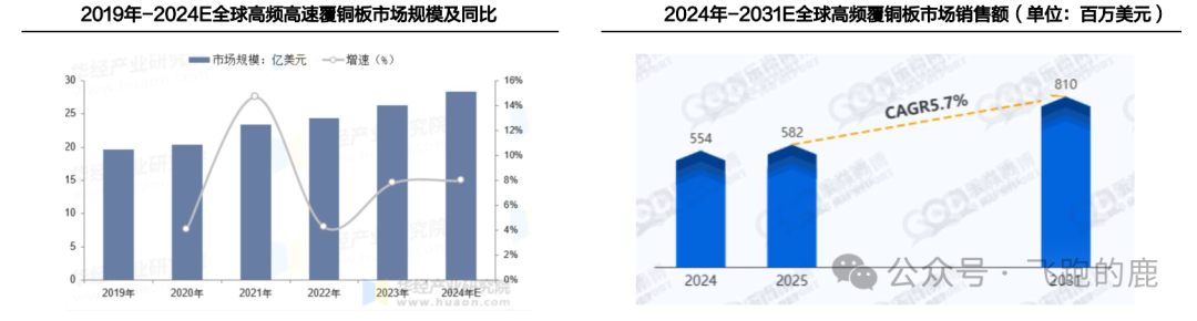
High-frequency high-speed copper clad laminates are growing faster than the entire copper clad laminate industry, driven by upgrades in base stations and core network servers. With the advent of the 5G era, antennas/radio frequency modules for macro and micro base stations, as well as optical communication modules and new packaging processes, will increasingly use these materials. According to Huajing Intelligence, the global high-frequency high-speed copper clad laminate market size is $2.63 billion in 2023, expected to reach $2.8 billion in 2024, with a year-on-year growth of about 8%.
As 5G networks expand and the number of smart driving vehicles increases, the high-frequency copper clad laminate industry will have even greater potential. According to Jianleshangbo (168Report), global sales of high-frequency copper clad laminates are expected to reach $554 million in 2024 and $810 million by 2031, with a compound annual growth rate of 5.7% from 2025 to 2031.
06 Electronic Resins
Electronic resins are equivalent to specialized “functional adhesives” in the electronics industry, meeting strict requirements for purity, performance, and stability, primarily used for copper clad laminates, semiconductor packaging materials, PCB inks, electronic adhesives, etc., with the core functions of insulation and adhesion.
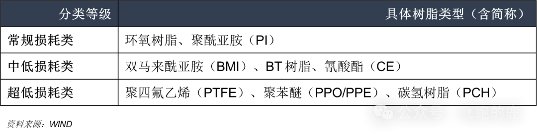
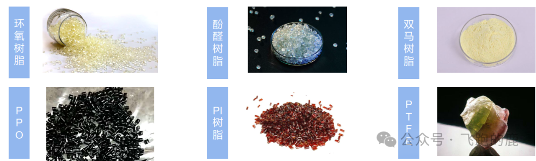
The electronic resins used in copper clad laminates are classified into three categories based on dielectric properties:
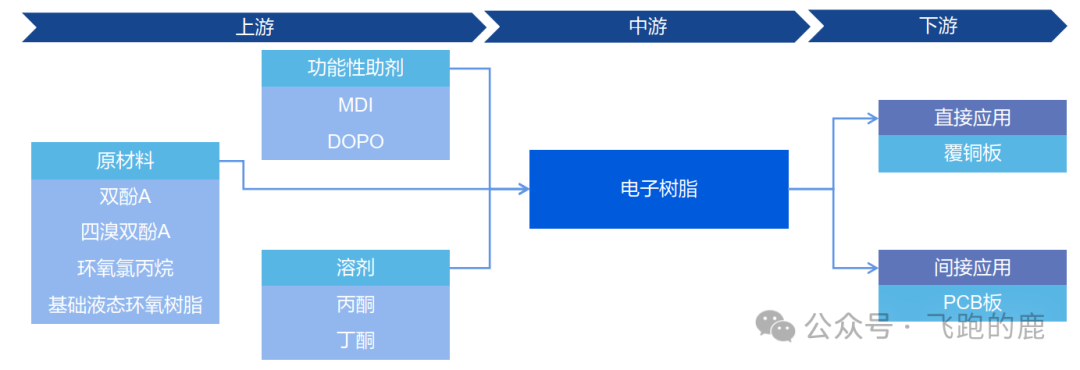
The electronic resin industry chain has clear divisions of labor: upstream includes raw materials such as bisphenol A, epoxy chloropropane, functional additives like MDI and DOPO, and solvents like acetone and methyl ethyl ketone, responsible for “supply”; midstream involves the production and manufacturing of electronic resins, which is the “processing stage”; downstream connects with the copper clad laminate industry, indirectly supplying PCBs, ultimately landing in end-user fields such as computers, consumer electronics, automotive electronics, and communication equipment.
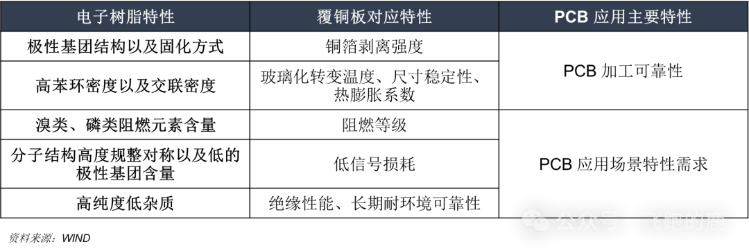
Electronic resins act as “characteristic regulators” for copper clad laminates—different resins can enhance different characteristics of copper clad laminates, and upgrades in copper clad laminate characteristics will further improve PCB performance. For example, the polarity group structure and curing method of the resin can affect the copper foil peel strength and interlayer adhesion of the copper clad laminate, making PCB processing more reliable; the more bromine and phosphorus flame-retardant elements in the resin, the higher the flame-retardant rating of the copper clad laminate; the more orderly the molecular structure of the resin and the fewer polar groups, the less signal loss in the copper clad laminate, making it suitable for high-speed and high-frequency communication scenarios, meeting the diverse application needs of PCBs.
Electronic-grade epoxy resin
Electronic-grade epoxy resin is one of the “core building materials” for high-performance copper clad laminates, with good mechanical properties, strong adhesion, high insulation, and heat resistance advantages, small shrinkage after curing, and not prone to cracking; special structures can also achieve low dielectric and intrinsic flame retardancy, meeting the demands for high-frequency signal transmission and high-speed information processing, widely used in next-generation servers, automotive electronics, communication networks, and other fields.
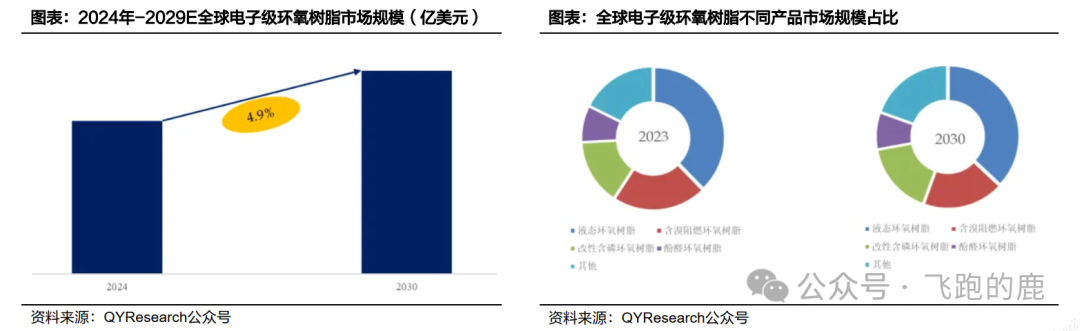
Demand for electronic-grade epoxy resin is expected to grow rapidly, with QYResearch estimating the global market size to be around $2.4 billion in 2024, expected to reach $3.22 billion by 2030, with a CAGR of 4.9% from 2024 to 2030.
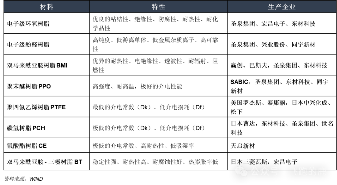
Currently, the companies producing resins are listed as follows:
07 Silica Powder
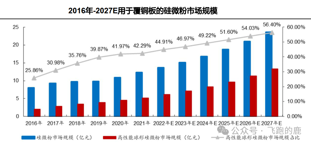
Silica powder is made from crystalline quartz and fused quartz as raw materials, processed through grinding, classification, impurity removal, and high-temperature spheroidization, belonging to non-toxic and odorless silicon dioxide powder.It is equivalent to a “high-performance functional filler” in the inorganic non-metallic field, possessing advantages of high heat resistance, high insulation, low expansion, and good thermal conductivity.
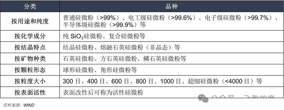
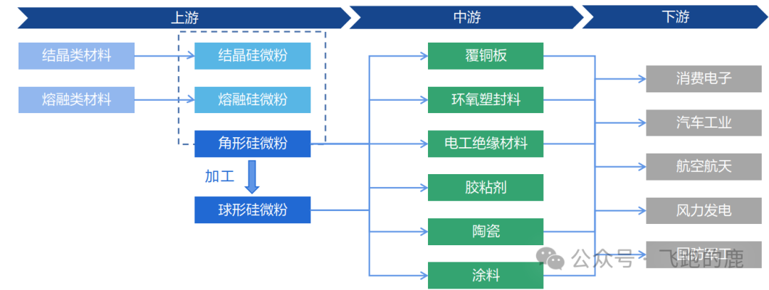
Silica powder is classified into angular and spherical types based on particle shape, widely used in copper clad laminates, chip epoxy encapsulants, insulating materials, adhesives, etc., with end applications in consumer electronics, automotive, aerospace, and wind power industries. Its industry chain is as follows:
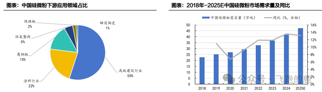
According to Huajing Intelligence, in the downstream applications of silica powder, high-grade building materials account for 55.1%, coatings account for 21.7%, copper clad laminates account for 15.1%, and epoxy encapsulants account for 4.9%.
The electronics industry is advancing towards high precision and sophistication, increasing the requirements for silica powder in copper clad laminates, driving market growth. According to Beizhesi Consulting, the demand for silica powder in China is expected to reach 418,000 tons in 2024, and 473,000 tons in 2025, with a year-on-year increase of 13.2%.
Among the inorganic functional powders used in copper clad laminates, silica powder has the widest application. For copper clad laminates that require dielectric properties and dielectric loss, modified silica powder that meets particle size and purity standards is selected—it can improve the expansion coefficient and thermal conductivity of PCBs, enhancing the reliability and heat dissipation of electronic products.
With the upgrade of terminal devices and the increase in AI server applications, the future demand for silica powder in copper clad laminates will rise rapidly.
08 Prepreg
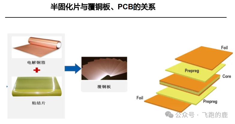
Prepreg (PP, also known as bonding sheet or adhesive film) serves as the “insulating interlayer” for PCBs—it is sandwiched between the core board and copper foil or between two core boards, acting as a dielectric layer for insulation, primarily composed of fiberglass cloth, resin, and curing agents.
It is a precursor product of copper clad laminates, made by soaking fiberglass cloth in resin, which is then reacted to form a solid resin that is not fully cured; during the lamination process, the core board, PP, and copper foil are stacked according to design, and under heat and pressure, the resin of the PP bonds adjacent layers, slowly curing through cross-linking to ultimately form.
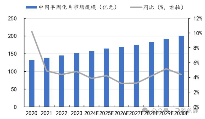
Demand growth driven by downstream industries such as AI, servers, and consumer electronics is leading to an upward trend in the prepreg market size. According to Zhiyan Consulting, the market size of prepregs in China was 15.192 billion yuan in 2023, expected to reach 20.044 billion yuan by 2030, with a CAGR of 4.0% from 2023 to 2030.
09 Electronic-Grade Fiberglass Cloth
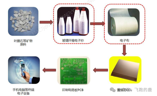
Electronic-grade fiberglass cloth (referred to as electronic-grade fiberglass) serves as the “insulating skeleton” for copper clad laminates— woven from single filaments with a diameter of less than 9μm, primarily used as an insulation reinforcement material for copper clad laminates, ultimately applied in various end electronic products.
Electronic-grade fiberglass cloth has high technical and financial barriers, with strong value creation capabilities across the entire industry chain, enabling substrates to possess excellent electrical properties and mechanical strength. The booming development of global 5G and consumer electronics markets is driving the copper clad laminate and PCB industries towards a broad prospect, which will also drive growth in the electronic-grade fiberglass cloth industry.
10 Conclusion
PCBs are the “core framework” of electronic devices, and in 2024, the demand for AI + downstream consumer electronics / 5G / servers is expected to explode, leading to an upward trend in the industry, with potential for both volume and price increases. HDI and 18+ layer multilayer boards are expected to benefit, with Prismark predicting a CAGR of 6.4% and 15.7% for global output value from 2024 to 2029, respectively.
Copper clad laminates are the core substrate of PCBs, evolving towards high-frequency and high-speed applications, with copper foil, resin, and fiberglass cloth as key raw materials; according to Zhongshang Intelligence (2025/05), they account for about 27% of PCB costs, with high growth in AI/5G demand.
Electronic resins influence the performance of copper clad laminates, driven by AI upgrades, with domestic promotion of local alternatives, and PTFE resins may become a trend.
Silica powder is used in copper clad laminates, with downstream upgrades + AI servers driving demand; Beizhesi Consulting predicts that demand in China will reach 473,000 tons in 2025 (up 13.2% year-on-year).
Scan below to join directly: