On April 11, 2024, the China Semiconductor Industry Association issued an “Emergency Notice on Clarifying the Certification Rules for the Origin of Semiconductor Products” (Zhongbanxie [2024] No. 12) to the entire industry. This document addresses the current disputes over the traceability of the semiconductor supply chain in the context of international trade frictions and establishes the following core regulations:
1. Legalization of Certification Standards
Strictly follow the relevant provisions of the General Administration of Customs’ “Management Measures for the Origin of Import and Export Goods” and adopt the principle of “substantial transformation of the four-digit tariff code” for integrated circuits (under HS code 8542), which means that the actual completion location of the wafer manufacturing core process—”tape-out”—will be used as the basis for determining the origin.
2. Declaration Operational Details
It is clearly required that enterprises, when importing and declaring customs:
• For finished integrated circuits that have been packaged, the origin declaration must trace back to the registered location of the wafer tape-out factory.
• For unpackaged wafer semi-finished products, the declaration should be made directly based on the country/region where the tape-out processing occurs.
• This move will cover all categories of semiconductor products, including logic chips, memory chips, and analog chips.
3. Strengthened Traceability Requirements
Enterprises must provide complete proof documents of the wafer factory’s tape-out process in the customs declaration documents, including:
• A manufacturing process statement issued by the tape-out factory.
• Supporting materials for process node technical parameters.
• Third-party verification reports required by customs (if applicable).
In the current global semiconductor technology blockade, this rule locks in the core technology link of wafer manufacturing, which not only complies with the WTO’s “Agreement on Rules of Origin” technical neutrality principle but also effectively prevents trade control evasion through simple overseas packaging, establishing a standardized traceability system for China’s semiconductor industry to participate in international competition.
1. Chip Origin Rules
The chip origin rules are standards used in international trade to determine the “economic nationality” of chips, directly affecting tariffs, the applicability of trade agreements, export controls, and anti-dumping measures. The core lies in determining which links in the chip production process play a decisive role in the “nationality” of the final product. The chip origin rules are a complex issue intertwined with technology, law, and geopolitics, requiring enterprises to comprehensively assess based on international trade agreements, domestic laws of various countries, and export control policies. As global semiconductor competition intensifies, origin determination may become one of the key tools in trade wars.
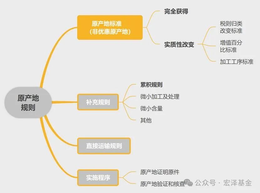
1 General Types of Origin Rules
Complete acquisition standard: Applicable only to products produced entirely in a single country (e.g., ore mining), but chips rarely meet this standard.
Substantial transformation standard: More common, divided into two categories:
Tariff classification change (HS Code change): If production leads to a change in the customs code of the product (e.g., from wafer to chip), it is considered of origin.
Value-added ratio: Requires a specific country’s contribution to the value-added ratio (e.g., above 35%-50%). For example, the U.S. requires a “local value-added ≥60%” for certain products.
Specific processing steps: Key steps (e.g., photolithography, etching) completed in a certain country are recognized as the origin of that country.
2 Special Characteristics of the Chip Industry
The chip industry chain is highly globalized, involving division of labor across multiple countries:
Design: United States (EDA software), China (some design companies).
Manufacturing: Taiwan, China (TSMC), South Korea (Samsung), United States (Intel).
Packaging and testing: Mainland China, Southeast Asia.
Raw materials/equipment: Japan (photoresist), Netherlands (ASML lithography machines).
Origin dispute points:
If a chip is designed in the U.S., manufactured in Taiwan, and packaged in Malaysia, how is the origin determined? Different countries may make different determinations based on the manufacturing link (Taiwan), value ratio (U.S. technology ratio), or final processing location (Malaysia).
3 Differences in Rules Among Major Countries/Regions
United States:
Emphasizes “substantial transformation,” but may adopt a “control standard” for high-tech products (e.g., technology source, intellectual property ownership).
In export controls, even if chips are produced overseas, if U.S. technology is used above a certain proportion (e.g., “25% rule” or stricter “10% rule”), they are still subject to U.S. restrictions.
European Union:
Adopts the principle of “last substantial processing,” focusing on the geographical location of the production link.
If wafer manufacturing or key processes are completed in the EU, they may be recognized as EU origin.
China:
Based on the “Regulations on the Origin of Import and Export Goods of the People’s Republic of China,” the standard is based on “last substantial processing” and value-added exceeding 30%.
For the semiconductor industry, it may tend to consider high-value links such as packaging and testing.
4 Special Rules in Trade Agreements
USMCA (United States-Mexico-Canada Agreement): Requires that 75% of automotive chips’ components be produced in North America to enjoy tax exemptions.
RCEP (Regional Comprehensive Economic Partnership): Adopts regional accumulation rules, allowing member countries to jointly share the value-added ratio. For example, the chip production links of China, Japan, and South Korea can be combined to calculate origin qualification.
5 The Relationship Between Export Controls and Origin Rules
Case: In the U.S. sanctions against Huawei, even if chips are manufactured in Taiwan, if U.S. technology or software design is used, exports to Huawei are still prohibited. At this time, origin rules and export controls (based on technology source) work together.
Long-arm jurisdiction: The U.S. includes foreign products containing U.S. technology/components under control through the “Export Administration Regulations” (EAR), exceeding the traditional origin rules.
6 Corporate Compliance Recommendations
Supply chain transparency: Track the physical location and technology source of each link in chip design, manufacturing, and packaging.
Cost optimization: Utilize the accumulation rules in trade agreements (e.g., RCEP) to reduce tariffs.
Risk avoidance: Assess whether the technology ratio meets control thresholds in response to export controls (e.g., U.S. BIS list).
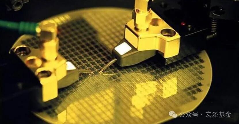
2. What is Tape-out
Tape-out is a critical step in the semiconductor chip manufacturing process, referring to the submission of completed integrated circuit (IC) layout data to a wafer foundry, where the first physical chips are produced through processes such as photolithography and etching. The core purpose is to verify the feasibility and functionality of the chip design, marking the transition from “design” to “mass production.”
Tape-out’s Core Logic
1 Ultimate Test of Design Verification
Chip designs must undergo simulation verification (using EDA tools), but only tape-out can truly expose physical layer issues (such as signal interference, abnormal power consumption, etc.).
Analogy: Just as architectural blueprints must be physically constructed to discover structural defects.
2 Extremely High Trial-and-Error Costs
High costs: A single advanced process (e.g., 5nm) tape-out can cost tens of millions of dollars, involving mask production, wafer processing, etc.
Long time cycle: From design submission to tape-out result feedback usually takes 3-6 months; if it fails, redesign is required (referred to as “re-tape-out”).
Tape-out’s Specific Process
1 Design Freeze
The chip design team completes the final layout (GDSII file) and passes design rule checks (DRC) and electrical rule checks (LVS).
2 Mask Fabrication
Based on the layout, photomasks are produced (similar to photographic negatives); a 7nm process requires 80-100 layers of masks, accounting for 30%-50% of the total tape-out cost.
3 Wafer Processing
The wafer foundry (e.g., TSMC, SMIC) performs hundreds of processes such as photolithography, etching, ion implantation, and deposition to form the physical chip structure.
4 Testing and Analysis
Functional testing, performance analysis, and defect inspection are conducted on the first batch of wafer samples to confirm whether they meet design specifications.
Tape-out Risks and Challenges
Technical risks:
Physical effects of advanced processes (e.g., 3nm) such as quantum tunneling and thermal noise may lead to discrepancies between design simulations and tape-out results.
Case: A certain GPU chip had to be redesigned after tape-out due to a clock tree design defect that caused power consumption to exceed the limit by 40%.
Commercial risks:
Tape-out failure may delay product launches, missing market windows (e.g., mobile chips missing flagship model release cycles).
Tape-out’s Common Scenarios
1 New Chip Development
Complex chips such as CPUs and GPUs typically require 2-3 tape-outs (engineering samples → mass production verification).
2 Process Verification
Wafer foundries provide “risk trial tape-outs” for new processes (e.g., SMIC N+1 process) for customers to test process compatibility.
3 Pilot Run
Before formal mass production, small batch tape-outs are conducted to verify yield and stability.
Industry Trend: Improving Tape-out Efficiency
Virtual Tape-out:
Utilizing cloud computing and AI to accelerate simulations, predicting tape-out issues in advance (e.g., Synopsys’s DSO.ai tool can reduce iteration times by 30%).
Multi-Project Wafer (MPW):
Multiple companies share mask costs, lowering the tape-out threshold for small and medium-sized manufacturers (common in mature processes above 28nm).
Tape-out is the “threshold of life and death” in the chip industry, directly determining product success or failure. As process evolution and design complexity increase, tape-out has evolved from a simple technical verification to a system engineering process that spans the entire chip development cycle, requiring collaboration among design, manufacturing, and testing resources.
U.S. Origin of 20 Semiconductor Companies
1. IDM (Integrated Device Manufacturer)
(1) Intel
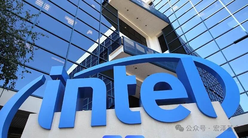
1 Basic Overview
Founded in 1968, headquartered in Santa Clara, California, USA.
Industry Position: One of the largest semiconductor companies in the world, focusing on CPUs, data center chips, and artificial intelligence technology. In 2024, revenue reached $12.7 billion (first quarter), but the annual net loss was $18.8 billion.
Strategic Transformation: Transitioning from traditional PC processors to data-centric businesses, focusing on AI, 5G, cloud computing, and promoting the IDM2.0 strategy (integrating design and manufacturing).
Global Layout: Manufacturing and R&D centers in the U.S., China (Shanghai, Chengdu, Dalian), Israel, etc. In 2024, acquired Tower Semiconductor in Israel to expand foundry capabilities.
2 Product Types
Intel’s product line covers multiple fields:
(1) Core Processors:
Client Computing: Core series (e.g., 14th generation Core), Pentium series.
Data Center and AI: Xeon processors, Falcon Shores/Jaguar Shores AI chips (under development).
(2) Semiconductor Manufacturing Services: Providing third-party chip foundry services through Intel Foundry Services (IFS), covering advanced processes (e.g., 18A process) and mature nodes.
(3) Other Products:
Internet of Things (IoT) solutions;
Non-volatile storage (e.g., solid-state drives);
Programmable solutions (FPGA) and autonomous driving technology (Mobileye division).
3 Main Origin and Supply Chain
According to China’s revised semiconductor origin rules in 2025, the origin standard is based on “wafer tape-out location.”
Intel’s product origin: Mainly completed wafer manufacturing in the U.S. (e.g., factories in Arizona, Ohio), with packaging and testing possibly distributed in Malaysia, but the origin is still recognized as the U.S.
Supply Chain Characteristics:
Vertical integration model (IDM): Independently completing design, manufacturing, and testing, competing with foundries like TSMC.
Global division of labor: Design relies on the U.S. headquarters, manufacturing is centered in the U.S., and packaging/testing is dispersed in Asia.
As a semiconductor industry giant, Intel is facing dual challenges of technological transformation and geopolitical issues. Its U.S.-based manufacturing model is at a disadvantage in tariff wars, while competitors are mitigating risks through foundry models. In the future, Intel needs to strengthen foundry services through the IDM2.0 strategy, accelerate technological iteration, and adjust its global supply chain layout to respond to market changes.
(2) Texas Instruments (TI)
1 Basic Overview
Texas Instruments was founded in 1930, originally as a geophysical service company (GSI), and transformed into a semiconductor company in 1951, headquartered in Dallas, Texas, USA. The company focuses on digital signal processors (DSP) and analog circuit technology, and is now one of the top ten semiconductor manufacturers globally, with revenue reaching $18.34 billion in 2021.
Technological Milestones: Launched the first commercial silicon transistor in 1954, invented the integrated circuit (Jack Kilby) in 1958, invented the handheld calculator in 1967, and developed digital light processing (DLP) technology in 1987.
Acquisition Strategy: In 2011, acquired National Semiconductor for $6.5 billion, consolidating its leadership in the analog chip market.
Leading position in the global analog circuit market, long-term leader in the digital signal processor (DSP) field.
Customers cover over 100,000 companies, with about 50% of mobile phones using its chips.
2 Product Types
Texas Instruments’ product line focuses on analog and embedded processing, covering a wide range of fields:
(1) Analog Chips (accounting for over 80% of revenue)
Power management (e.g., battery management IC, DC-DC converters)
Data converters (ADC/DAC), amplifiers, interface chips
(2) Embedded Processors
Microcontrollers (MCU), digital signal processors (DSP)
Automotive electronic processors (e.g., ADAS system chips)
(3) Sensors and Control Systems
Temperature sensors, magnetic field sensors, millimeter-wave radar sensors (for automotive and industrial applications)
(4) Other Innovative Products
DLP projection technology (for cinema and industrial projection)
Educational technology products (e.g., graphing calculators TI-81)
3 Main Origin and Manufacturing Layout
According to semiconductor industry practices, the origin is usually based on the wafer manufacturing location. Texas Instruments’ core manufacturing links are concentrated in the U.S. and some overseas factories.
Global Manufacturing Bases
U.S.: Dallas (headquarters), Lehi, Utah (12-inch wafer factory), new factory built in 2022.
Asia: Chengdu, China (wafer manufacturing and testing), Baguio City, Philippines (testing).
Europe: Avezzano, Italy (wafer manufacturing).
4 Supply Chain Characteristics
(1) Vertical Integration Model (IDM)
Independently completing the entire process of chip design, manufacturing, and testing, forming differentiated competition with foundries like TSMC.
In 2021, invested $30 billion to expand U.S. wafer factories, strengthening advanced process (e.g., 45nm-130nm analog chip) capacity.
(2) Global Supply Chain Network
Raw materials: Collaborating with Japan’s Shin-Etsu Chemical (photoresist), Netherlands’ ASML (lithography machines).
Packaging and testing: Relying on Asian factories (e.g., Philippines, Malaysia) to reduce costs.
Logistics and distribution: Covering customer needs through sales agencies in over 30 countries worldwide.
(3) Strategic Adjustments
In 2024, received $1.6 billion in subsidies from the U.S. government to accelerate domestic capacity construction to address geopolitical risks.
Gradually exiting the consumer electronics field, focusing on high-profit markets such as industrial and automotive.
Texas Instruments, with its leading position in analog chips and embedded processing technology, has built a complete supply chain covering design, manufacturing, and testing. Its core manufacturing bases are concentrated in the U.S., while optimizing costs through Asian factories. In the future, as semiconductor industry competition intensifies, TI’s strategic focus will shift towards high-reliability industrial chips and automotive electronics, enhancing supply chain resilience through localized capacity.
(3) Micron Technology
1 Basic Overview
Micron Technology, Inc. was founded in 1978, headquartered in Boise, Idaho, USA, by Ward Parkinson, Joe Parkinson, Dennis Wilson, and Doug Pitman. The company initially started as a semiconductor design consultancy and established its first wafer manufacturing plant (Fab1) in 1981, officially entering the semiconductor manufacturing field.
Industry Position: One of the largest semiconductor memory and imaging product manufacturers globally, focusing on DRAM, NAND flash, etc. In 2023, revenue reached $30.758 billion, ranking 127th in Fortune’s U.S. 500.
Global Layout: R&D centers and manufacturing bases in Asia, Europe, and the Americas, with over 43,000 employees. The Xi’an factory in China is its core production base in China.
Expanding from traditional memory chips to high-performance computing and artificial intelligence fields, launching PCIe 6.0 data center SSD technology in 2024, with sequential read bandwidth exceeding 26GB/s.
Through acquisitions (e.g., acquiring Japan’s Elpida in 2012, holding Taiwan’s Inotera in 2016), it has strengthened its market share, consolidating its position as the third-largest player in the DRAM market (after Samsung and SK Hynix).
2 Product Types
Micron’s product line focuses on memory chips, covering multiple application fields:
(1) DRAM (Dynamic Random Access Memory)
Used in servers, PCs, smartphones, etc. In 2022, launched automotive-grade LPDDR5 DRAM, applied in smart cars like Ideal L9.
(2) NAND Flash
Includes SSD solid-state drives (e.g., 5210 ION series), UFS storage cards, etc. In 2023, launched 176-layer 3D NAND chips, improving storage density and energy efficiency.
(3) NOR Flash
Mainly used for embedded system code storage, such as industrial control devices.
(4) CMOS Image Sensors
Applied in mobile phones, security cameras, etc. In 2008, spun off as a separate company Aptina (later acquired by ON Semiconductor).
(5) Other Products
Memory modules, data center solutions, and advanced packaging products based on 3D Fabric technology.
3 Main Origin
(1) Manufacturing Base Distribution
U.S. domestic: Core wafer manufacturing concentrated in Boise, Idaho, Utah, etc. In 2022, announced a $15 billion investment to build a new memory chip factory in Boise.
Asia:
Xi’an, China: Established in 2007, mainly engaged in packaging testing and memory module assembly. In 2024, expansion project initiated, with total investment exceeding 4.3 billion RMB.
Hiroshima, Japan: DRAM production base, introduced EUV lithography technology in 2022 to produce cutting-edge products.
India: Approved in 2023 to invest $1 billion to build an ATMP (Assembly, Testing, Marking, and Packaging) factory.
Europe: Previously operated a wafer factory in Avezzano, Italy, later sold and transformed.
(2) Origin Determination Rules
According to semiconductor industry practices, the origin is usually based on the wafer manufacturing location. Micron’s high-end DRAM and NAND chips are mainly manufactured in the U.S., with packaging and testing dispersed in Asia.
4 Supply Chain Characteristics
(1) Vertical Integration Model (IDM)
Independently controlling the entire process of design, manufacturing, and testing, forming differentiated competition with foundries like TSMC.
In 2024, received $13.6 billion in subsidies from the U.S. government to accelerate domestic capacity expansion to address geopolitical risks.
(2) Global Supply Chain Network
Raw materials: Relying on Japan’s Shin-Etsu Chemical (photoresist), Netherlands’ ASML (lithography machines), etc.
Packaging and testing: Mainly handled by Asian factories (Xi’an, Malaysia, Philippines) for low-cost packaging.
(3) Risks and Adjustments
Geopolitical impact: In 2023, China banned the procurement of Micron products for key information infrastructure due to “national security risks,” accelerating its layout in India and U.S. domestic capacity.
Technological competition: Facing technological suppression from Samsung, SK Hynix, and patent litigation challenges from Chinese companies like Yangtze Memory Technologies (YMTC).
2. Fabless (Fabless Design Companies)
(4) NVIDIA
1 Basic Overview
Since its establishment in 1993, NVIDIA has stood at the forefront of technological waves, headquartered in the innovation hub of California. After nearly thirty years of deep cultivation and breakthroughs, the company has built a full-stack computing ecosystem covering CPUs, DPUs, GPUs, and AI software, with business extensions from gaming entertainment to data centers, professional visualization, and autonomous driving, continuously leading the industrial transformation of artificial intelligence and high-performance computing.
With its disruptive architectural innovations and ecosystem integration capabilities, NVIDIA has firmly established itself as the absolute leader in the global AI chip market, creating insurmountable industry barriers. In the data center field, its solutions have surpassed a 90% market share, demonstrating deep control over the explosive growth of computing power demand. The capital market has also fully recognized its value, with the company’s market capitalization exceeding 11 trillion yuan, making it an undeniable “giant” in the global technology landscape, equivalent to the total of the two leading global foundries, TSMC, showcasing its extraordinary dominance in the intersection of semiconductors and artificial intelligence.
2 Product Types
Data center GPUs, consumer-grade GPUs, automotive chips, edge AI chips
3 Main Origin
Wafer production in Taiwan, South Korea, the U.S., and Singapore, with packaging in Southeast Asia.
4 Supply Chain Challenges:
Impacted by international trade policies (e.g., export restrictions to China), NVIDIA needs to adjust its supply chain layout while addressing the global shortage of chips like H100/A100.
(5) Qualcomm
1 Basic Overview
As a global leader in communication technology and semiconductor solutions, Qualcomm has been sailing since 1985 in San Diego, USA. After more than thirty years of technological accumulation, it has grown into a multinational technology giant with a market value of $157.6 billion (2023 data), employing over 40,000 people and building a complete ecosystem covering R&D, manufacturing, and commercialization. The company’s core patent matrix spans key wireless communication standards such as CDMA and 5G, holding over 140,000 patent technologies, creating the industry’s most comprehensive standard-essential patent (SEP) portfolio, forming an insurmountable technological moat.
The flagship Snapdragon mobile platform has long dominated the high-end Android market, driving over 1 billion smartphones globally to achieve intelligent leaps in 2023. Its technology licensing business (QTL) further outputs patent value to over 300 companies worldwide, building a sustainable innovation flywheel of “R&D – Patent – Licensing.” In the 5G era, Qualcomm leads the commercial wave with groundbreaking baseband chips like X50, while simultaneously expanding into new tracks such as AI, IoT, and automotive electronics. The fourth-generation Snapdragon 8s Gen4 processor, set to launch in 2025, aims to penetrate the mid-range market with outstanding performance, showcasing a vision of technological inclusivity.
Its unique “chip + patent” dual-driven business model allows patent licensing revenue to continuously contribute over 30% of revenue, but it has also raised regulatory concerns in multiple countries due to technology monopoly disputes (e.g., a $6.088 billion antitrust fine in China). Nevertheless, Qualcomm remains among the top ten global semiconductor companies, continuously defining the boundaries of future communication and intelligent computing through technological innovation.
2 Supply Chain and Challenges
The supply chain relies on TSMC for 4nm chip foundry, with packaging dependent on ASE (Taiwan);
Snapdragon chips packaged in Taiwan are exempt from additional tariffs, while automotive chips manufactured in U.S. factories may be affected.
(6) AMD (Advanced Micro Devices)
1 Basic Overview:
Founded in 1969, headquartered in Sunnyvale/Santa Clara, California, USA, by Jerry Sanders. The company is a global leader in semiconductors, focusing on CPU, GPU, and APU computing solutions, covering gaming, AI, cloud computing, and data centers.
Entered the microprocessor market in 1975, competing with Intel by launching classic products like Am286 and Am386; acquired ATI in 2006, becoming a vendor with both CPU and GPU; in 2017, achieved commercial recovery with the “Ryzen” series processors, now led by CEO Dr. Lisa Su, transforming into a leader in high-performance and adaptive computing.
2 Product Types:
Ryzen series: Consumer-grade star products covering entry-level (Ryzen 3), mainstream (Ryzen 5), and high-end (Ryzen 7/9) markets, such as Ryzen 9 5950X (16 cores, 32 threads, boost frequency 4.9GHz);
Threadripper: Targeting high-end gamers, content creators, and workstations, such as 3990X (64 cores, 128 threads);
EPYC: Core product in the server field, supporting cloud computing and large-scale data processing in data centers.
GPU series:
Radeon: Covering gaming graphics cards (e.g., RX 7900 XTX), professional graphics cards (Radeon PRO), embedded and semi-custom solutions.
APU series:
Integrating CPU and GPU functions, suitable for thin and light laptops and low-power devices.
3 Main Origin and Supply Chain:
Manufacturing Layout:
U.S. domestic: New factory to be put into production in 2025, focusing on AI chip tape-out;
Taiwan: Main chip tape-out location, relying on TSMC and other foundries for advanced processes (e.g., 5nm/4nm).
Supply Chain Management:
Global supplier network: Covering wafer manufacturing, bump processing, packaging testing, etc., to ensure large-scale production needs;
Quality standards: Suppliers must pass ISO 9001 certification, using 8D problem-solving methods and DMAIC continuous improvement processes;
Risk control: Establishing business continuity plans to respond to market fluctuations, ensuring long-term supply stability.
4 Supply Chain Challenges:
Relying on foundries like TSMC, balancing capacity allocation with geopolitical risks;AI chip field competing directly with NVIDIA, requiring continuous R&D investment to solidify its position.
(7) Broadcom
1 Basic Overview
Founded in 1991 (formerly known as Avago Technologies), headquartered in Palo Alto, California; core business includes network chips, storage controllers; currently the largest wired communication chip manufacturer globally.
2 Product Types
Data center ASIC/switching chips, 5G/WiFi 7 communication chips, RF front-end modules, automotive electronic chips, IoT modules.
3 Industry Layout
Wafer assembly in Taiwan, South Korea, the U.S., Germany; packaging in mainland China, Taiwan, Southeast Asia, Singapore.
4 Supply Chain Management
Supply chain: TSMC foundry for 7nm/5nm wafers, packaging concentrated in Singapore;
Tariff impact: If the value added in Singapore packaging exceeds 30%, the origin is Singapore, exempt from additional tariffs.
3. Semiconductor Equipment and Materials
(8) Applied Materials
1 Basic Overview
Founded in 1967, headquartered in Santa Clara, California; core business includes wafer manufacturing equipment (deposition, etching); the largest semiconductor equipment supplier globally, with a market share exceeding 20%!
2 Supply Chain Management
Supply chain: R&D in Silicon Valley, production bases distributed in China, Malaysia;
Tariff impact: Equipment produced in the U.S. is subject to a 125% tax rate, and anti-dumping duties may be even higher.
(9) Lam Research
1 Basic Overview
Founded in 1980, headquartered in Fremont, California; core business includes semiconductor etching and thin film deposition equipment; currently the second-largest semiconductor equipment supplier, with a market share of 35% in etching equipment.
2 Supply Chain & Tariff Impact
Supply chain: R&D in the U.S., manufacturing relies on Taiwan and South Korea;
Tariff impact: Equipment from U.S. factories is subject to additional tariffs, and products from overseas foundries must be determined based on value-added ratios.
(10) KLA
1 Basic Overview:
Founded in 1975, headquartered in Milpitas, California; core business includes wafer inspection equipment; currently the global leader in inspection equipment, with a market share exceeding 50%.
2 Supply Chain & Tariff Impact:
Supply chain: R&D in the U.S., production bases distributed in China, Israel;
Tariff impact: Equipment produced in U.S. factories is subject to an 84% tax rate, and products from overseas foundries that do not meet the 30% value-added requirement are still considered U.S. origin.
4. Analog and Power Semiconductors
(11) Analog Devices (ADI)
1 Basic Overview:
This semiconductor industry pioneer has been headquartered in Norwood, Massachusetts, USA, since its founding in 1965. As an outstanding representative in the high-performance analog chip field, the company focuses on the R&D and innovation of semiconductor sensors and signal processing integrated circuits (ICs), building a competitive advantage from design to application through deep technical accumulation and vertical integration capabilities.
In the technology-intensive field of analog chips, the company holds the second-largest market position globally, with its products demonstrating excellent performance advantages in key tracks such as industrial control and automotive electronics. Especially in the current booming development of industrial IoT and intelligent driving technology, the company continues to consolidate its leadership in industrial-grade and automotive-grade chips with high reliability and low power consumption solutions, becoming an important force driving semiconductor technology innovation and industrial upgrading.
2 Supply Chain & Tariff Impact:
Supply chain: Wafer factories in Washington and Oregon, with packaging and testing distributed in Thailand and Malaysia;
Tariff impact: Chips produced in the U.S. are subject to additional tariffs, and overseas packaging that does not meet the 30% value-added requirement is still considered U.S. origin.
(12) ON Semiconductor
1 Basic Overview:
Founded in 1999 (formerly Motorola Semiconductor), headquartered in Phoenix, Arizona; a leader in the global automotive CMOS image sensor (CIS) market, with a market share of 33%, and holds up to 68% in the ADAS sub-market. ON Semiconductor is also involved in millimeter-wave and laser radar technology, promoting multi-sensor fusion trends, enhancing its applications in autonomous driving and intelligent transportation systems; currently among the top ten global power device manufacturers, leading in automotive-grade silicon carbide (SiC) technology with a market share of 23.6%.
2 Supply Chain & Tariff Impact:
Supply chain: Wafer factories in New York and Arizona, with packaging and testing distributed in the Philippines and China;
Tariff impact: Products packaged in China that do not meet the 30% value-added requirement are still considered U.S. origin.
(13) Microchip Technology
1 Basic Overview:
Microchip Technology has been rooted in Chandler, Arizona, USA, since its establishment in 1989. As a deep cultivator in the semiconductor field, the company focuses on microcontrollers (MCUs) and field-programmable gate arrays (FPGAs), establishing its leading position in the global semiconductor industry through deep technical accumulation and forward-looking market layout.
Specifically, Microchip Technology firmly occupies the leading position in the 8-bit/16-bit MCU market, while also being a leading supplier of microcontroller and analog semiconductor solutions, continuously providing high-performance chip support for key fields such as automotive electronics, industrial control, and the Internet of Things. Notably, the company has further consolidated its industry position through strategic acquisitions—completing the integration of Atmel for $3.6 billion, not only expanding its product matrix and customer coverage but also initiating a new wave of consolidation in the semiconductor industry, demonstrating its strategic foresight in accelerating technological integration and market penetration through capital operations.
2 Supply Chain & Tariff Impact:
Supply chain: Wafer factories in Arizona and Oregon, with packaging and testing relying on third parties;
Tariff impact: Chips produced in the U.S. are subject to additional tariffs, and overseas foundry products must be determined based on value-added ratios.
5. RF and Communication Chips
(14) Skyworks Solutions
1 Basic Overview:
This leading RF technology company traces its roots back to 1962, originally as the RF department of Texas Instruments, and has been deeply engaged in the wireless communication field for over half a century. Now headquartered in Andover, Massachusetts, the company focuses on the R&D and manufacturing of RF front-end (RFFE) modules, providing critical technical support for diverse scenarios such as automotive electronics, broadband communication, cellular network infrastructure, energy management, industrial control, medical devices, defense, and mobile terminals.
With continuous innovation in RF chips, the company holds the third-largest position in the global industry, notably as a core partner in Apple’s supply chain. In 2023, revenue from Apple accounted for 66%, highlighting the deep binding of both parties in cutting-edge technology collaboration and market penetration. This strategic partnership not only validates the company’s excellence in RF technology but also indicates its continued key role in the 5G era and future wireless communication revolution.
2 Supply Chain & Tariff Impact:
Supply chain: U.S. domestic wafer factories, with packaging and testing distributed in Mexico and Costa Rica;
Tariff impact: If the value added in Mexican packaging does not meet 30%, the origin is still considered U.S., and additional tariffs must be paid.
(15) Qorvo
1 Basic Overview:
This leading RF technology company was born in 2015, formed by the merger of RFHIC and TriQuint, headquartered in the Greensboro technology corridor of North Carolina. The company focuses on the R&D and innovation of RF filters and power amplifiers, holding over 50% market share in the bulk acoustic wave (BAW) filter field, ranking second in the global RF chip market.
Its core product line includes high-performance switches, power amplifiers, and multi-band RF filters, widely used in global mobile communications, cellular networks, wireless local area networks (WLAN), cable television/broadband access (CATV/Broadband), as well as aerospace and defense. By providing highly integrated RF solutions, the company not only enhances the connectivity performance of mobile devices but also builds solid technical support for wireless infrastructure, defense communication systems, and satellite navigation, continuously driving the evolution and upgrade of global communication networks.
2 Supply Chain & Tariff Impact:
Supply chain: U.S. domestic wafer factories, with packaging and testing distributed in Costa Rica and China;
Tariff impact: If the value added in Chinese packaging does not meet 30%, the origin is still considered U.S.
6. Storage and Optoelectronics
(16) Western Digital

1 Basic Overview:
Since its establishment in 1970, the company has always set its strategic headquarters in the global technology innovation hub of San Jose, California. As a pioneer in the data storage field, the company focuses on mechanical hard drives (HDD) and solid-state drives (SSD), providing high-performance, high-reliability storage solutions for global personal computer and enterprise users.
After half a century of deep cultivation in the industry, Western Digital has firmly established itself as the second-largest player in the global storage market, with its products achieving industry-leading levels in capacity, speed, and durability. Notably, in September 2017, the company strategically acquired Toshiba’s semiconductor business for $18.3 billion, significantly expanding its flash memory technology landscape and further consolidating its competitive advantage in the solid-state drive field through the integration of Toshiba’s NAND flash technology. This milestone acquisition not only demonstrates Western Digital’s foresight in grasping technological trends but also opens a new chapter of growth in the global storage market.
2 Supply Chain & Tariff Impact:
Supply chain: U.S. domestic R&D, production bases distributed in China and Malaysia;
Tariff impact: Storage chips produced in U.S. factories are subject to additional tariffs, and overseas foundry products must be determined based on value-added ratios.
(17) Marvell

1 Basic Overview
This globally leading storage technology company was founded in 1995, registered in the internationally renowned offshore financial center of Bermuda, with its operational headquarters set in the technology hub of Santa Clara, California. The company focuses on storage controllers and network processors, becoming the leading provider of global storage chip interface solutions through continuous innovative R&D.
Its technological achievements are widely applied in enterprise storage systems, data centers, and high-performance computing platforms, significantly enhancing the overall performance and reliability of storage devices through efficient data transmission and access control solutions. This technological leadership not only stems from a profound understanding of storage architecture but also benefits from the company’s cross-innovation in the field of network processors, forming a unique competitive advantage that continuously leads the direction of storage technology innovation.
2 Supply Chain & Tariff Impact:
Supply chain: TSMC foundry for 7nm wafers, with packaging distributed in Taiwan and Singapore;
Tariff impact: If products packaged in Taiwan exceed 30% value-added, the origin is Taiwan, exempt from additional tariffs.
7. EDA and Design Tools
(18) Synopsys
1 Basic Overview:
Since its establishment in 1986, the company has always set its strategic headquarters in the forefront of global technological innovation—Mountain View, California. As a leading company in the field of electronic design automation (EDA), the company focuses on providing cutting-edge EDA software and intellectual property core (IP Core) solutions, holding approximately 35% market share, firmly establishing its position as the industry leader. Its technological achievements are widely applied throughout the chip design cycle, from early 386 architecture to the latest 2nm process AI chips, becoming an indispensable technical enabler in the global chip automation design field.
Synopsys not only provides the semiconductor industry with the most advanced design toolchain but also builds a complete solution for chip developers from front-end design to back-end verification through continuously innovative IP core technology. This combination of depth and breadth in technology means that top global chip manufacturers rely on the core technical support provided by Synopsys in their pursuit of performance limits and power consumption optimization. This strategic position not only highlights the company’s absolute leadership in the EDA field but also indicates its continued key role in the future evolution of semiconductor technology.
2 Supply Chain & Tariff Impact:
Supply chain: R&D in the U.S., technical support distributed in China and India;
Tariff impact: Software services are not directly affected by tariffs, but technology exports may be restricted.
(19) Cadence
1 Basic Overview:
Born in 1988 from a historic industry consolidation, formed by the merger of SDASystems and ECAD, headquartered in the global technology innovation center—San Jose, California. The company focuses on the development of EDA tools and AI chip design platforms, holding approximately 30% market share, ranking among the top three EDA companies globally, continuously pushing the boundaries of semiconductor design technology.
As an expert in electronic design automation, the company provides a complete toolchain solution from front-end design to back-end verification, empowering the chip design process with its depth of technology, especially in the field of AI chip design, showcasing forward-looking layouts. This accumulation of technology and strategic vision not only stems from a profound understanding of the essence of EDA technology but also benefits from the innovative spirit embedded in the company since its inception, ensuring its core position in the wave of technological iteration in the global semiconductor industry, providing indispensable technical support for global chip designers.
2 Supply Chain & Tariff Impact:
Supply chain: R&D in the U.S., technical support distributed in China and Japan;
Tariff impact: Software services are exempt from tariffs, but technology cooperation may be subject to export controls.
8. Acquired Companies (Historical Position)
(20) Xilinx (acquired by AMD)
1 Basic Overview:
Founded in 1984, headquartered in San Jose, California; the largest supplier of complete programmable logic solutions globally, with its core business in FPGAs and adaptive computing chips; before being acquired by AMD, it was the global leader in FPGAs; on July 18, 2018, Xilinx announced the acquisition of the AI chip star startup Deep Vision, known as the “Chinese NVIDIA.”
2 Supply Chain & Tariff Impact:
Supply chain: TSMC foundry for 7nm wafers, with testing undertaken by Tongfu Microelectronics (China);
Tariff impact: Products packaged in China that do not meet the 30% value-added requirement are still considered U.S. origin.
Domestic Corresponding Beneficiary Targets
1. Wafer Foundry Giants
- SMIC: As the flagship enterprise in the domestic semiconductor foundry field, its 8-inch and 12-inch wafer production capacity ranks among the top in the country and has taken the lead in breaking through the mass production of advanced processes below 28nm.
- Huahong Group: The global leader in smart card chip foundry, with power device manufacturing capabilities that are second to none globally, continuously consolidating its leading position in specialty processes.
2. IDM and Fabless Leading Enterprise Matrix
- China Resources Microelectronics: A leading enterprise in domestic MOSFET devices, with a complete IDM industrial chain layout, achieving full autonomy in power semiconductors, MEMS sensors, and photomask manufacturing.
- Silicon Motion: Deeply engaged in power semiconductors, IGBT, IPM modules, and optoelectronic devices, while simultaneously expanding into third-generation wide bandgap semiconductor technology.
- Star Semiconductor: A benchmark in IGBT module technology in China, with products widely used in new energy and industrial control fields.
3. Semiconductor Equipment Domestic Substitution Pioneers
- North Huachuang: Building a complete equipment matrix for etching, deposition, thermal treatment, and cleaning, leading the wave of domestic semiconductor equipment.
- SMEE: A high-end etching equipment technology breakthrough company, with products entering international advanced process production lines.
- Tuojing Technology: A leader in thin film deposition equipment, achieving mass production breakthroughs in hybrid bonding technology.
- Huahai Qingke: CMP equipment leader, simultaneously laying out thinning and cutting and cleaning equipment.
- Shengmei Shanghai: A leader in cleaning equipment technology, with significant progress in the development of plating and PECVD equipment.
- Xinyuan Micro: A pioneer in the localization of coating and developing equipment, breaking through key nodes in lithography processes.
- CASIC: A platform layout for measurement and testing equipment, with steadily increasing market share.
- Jingce Electronics: A pioneer in the field of flat panel display testing, deeply engaged in semiconductor testing equipment.
- Changchuan Technology: A technology breakthrough company in testing equipment, achieving domestic substitution of testing machines and sorting machines.
- Jingyi Equipment: An expert in semiconductor temperature control equipment, covering advanced processes and 3D NAND storage chip manufacturing.
4. Domestic Substitution Forces in the CPU Field
- Loongson Technology: A builder of the domestic CPU ecosystem, forming a complete basic software technology system.
- Hygon Information: A leading enterprise in x86 server CPU and accelerator technology.
5. Analog Chip and DSP Technology Cluster
- GigaDevice: Covering the entire signal chain and power management chip, with over 5200 products.
- Silergy: An extender of signal chain technology, laying out automotive electronics and power management fields.
- Guorui Technology: A benchmark for domestic DSP processor technology, serving the defense and communication fields.
6. Breakthroughs in the Full Chain of Storage Chips
- GigaDevice: A leader in NOR Flash and DRAM design, laying out SLC NAND and MCP storage solutions.
- Beijing Junzheng: A deep cultivator of automotive-grade storage technology, covering all types of storage chips.
- Dongxin Technology: An expert in small-capacity storage chips, focusing on SLC NAND and MCP solutions.
- Lanqi Technology: A global leader in DDR5 memory interface technology.
- Jiangbolong: A storage module technology integrator, collaborating with Yangtze Memory to create high-end storage solutions.
7. Automotive and Security CIS Technology Camp
- Weir Shares: Full coverage of CMOS image sensors, competing with overseas giants.
- SiTewi: Leading global shipments of security CIS, with automotive sensors recognized by manufacturers like BYD.
8. MCU and FPGA Technology Breakthroughs
- GigaDevice: A benchmark in 32-bit MCU technology, with the GD32 series competing with international mainstream products.
- Zhiyuan Electronics: An MCU expert for home appliances and automotive, with leading lithium battery management chip technology.
- Unisoc: A technology breakthrough in FPGA, serving the communication and data center fields.
9. RF Front-End Technology Cluster
- Zhuoshengwei: An expert in RF switches and LNA technology, serving the mobile terminal field.
- Weijie Chuangxin: A leading player in 5G RF front-end technology, laying out automotive electronics and AI terminals.
10. EDA Technology Domestic Substitution Pioneers
- Huada Jiutian: A leading domestic EDA software company, promoting independent innovation in the electronic design automation field.
* Disclaimer: The content of this article is for industry analysis reference only and does not constitute any investment advice!