Have you discovered the options for “Share” and “Like”? Click here to check it out.
Last Issue Review
From 0 to 1: A Comprehensive Breakdown of the SAW Wafer Fabrication Process (Part 1 – Photolithography)
Reshaping the Body – Thin Film Deposition
While beautiful appearances are commonplace, interesting souls are rare. In the life spectrum of Surface Acoustic Wave (SAW) filters, photolithography acts as the poet that gives it a soul, while thin film deposition forges its robust body. The three layers of precision films resemble the organic structure of a living organism:
1. Intelligent Core (IDT-M1 Metal Layer): Like neurons in the brain, the interdigitated electrodes are arranged to precisely control the pulse (frequency) of electromagnetic resonance, managing the rhythm of energy breathing (insertion loss and power tolerance), defining the oscillation source that embodies the device’s soul;
2. Energy Trunk (M2-Busbar Wiring Layer): Like an intricate steel body, it constructs low-resistance highways in the chip territory, taming currents in the hundred milliamp range, locking signal loss and thermal collapse risks in a cage, supporting the resilient backbone for high-power traffic;
3. Indestructible Armor (Passivation Layer): Transforming into a nano armor covering the surface, it uses chemical passivation to isolate against corrosive oxygen and moisture, forging a body that withstands humidity and aging for a decade.
When the seemingly ordinary thin film materials are precisely filled according to the definitions of photolithography, the SAW finally possesses both form and spirit, becoming a bare chip with acoustic resonance functions, which can then be packaged into RF chips, cutting through the communication world.
Introduction to Thin Film Growth Methods
Thin film epitaxy is a critical material preparation method widely used in semiconductor devices, optoelectronics, and nanotechnology. This process involves the layer-by-layer deposition of atoms or molecules onto a substrate surface, forming thin films with specific properties and structures. Therefore, the quality of the growth process directly affects the structure and final performance of the thin films. Coating can be broadly divided into two categories: Physical Vapor Deposition (PVD) (evaporation/sputtering), which relies on physical phase changes, and Chemical Vapor Deposition (CVD), which relies on chemical reactions. Evaporation coating is akin to boiling water, where the coating material (metal or compound) is heated in a vacuum environment, causing it to vaporize and sublime, with the vapor condensing on the substrate surface to form a thin film. Sputtering coating uses high-energy particles (such as argon ions) to bombard the target material’s surface, causing target atoms to be dislodged and deposited on the substrate surface under magnetic control. Chemical vapor deposition involves chemical reactions of gaseous precursors on the substrate surface (thermal decomposition/oxidation/reduction), generating solid thin film deposits. For low-melting-point metals (Al/Ag), evaporation coating is typically chosen, while certain high-melting-point targets (W/TiN) can only use sputtering coating. CVD is more versatile, applicable to various medium materials, high-melting-point materials/hard coatings, and functional films.
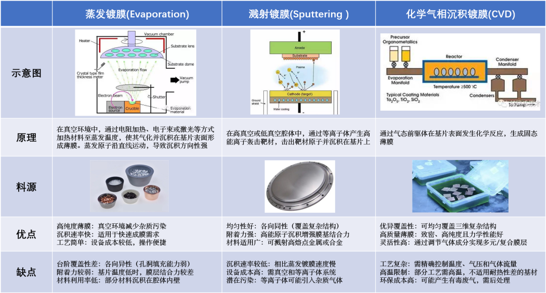
Figure 22: Principles, Advantages, and Disadvantages of Evaporation Coating, Sputtering Coating, and Chemical Vapor Deposition
Currently, in the technical route for manufacturing the M1 layer (IDT) of SAW, there are mainly two options: the Lift-off process and the Etch process. The Lift-off process is quite special; on one hand, due to the inherent properties of the photoresist, and on the other hand, the anisotropy of sputtering coating can lead to difficulties in lift-off, making it typically used in conjunction with evaporation coating. The Etch process allows for free selection of coating processes, and for product performance, sputtering coating is generally used in combination. Sputtering coating is derived from atomic deposition, so the crystallinity of the resulting metal film layer is usually better than that of evaporation coating. However, choosing sputtering coating requires the Etch process, which significantly increases costs, necessitating a choice between performance and cost. The M2 metal, due to its greater thickness and lower precision requirements, typically uses the cheaper evaporation coating process.

Figure 23: Comparison of Lift-off and Etch Processes
Metal Thin Film Materials for SAW
In the manufacturing of interdigitated transducers (IDT) for Surface Acoustic Wave (SAW) devices, Al is used as the main material due to its low density, good acoustic velocity matching, and extremely low resistivity (2.65μΩ·cm). However, due to the weak chemical bonding of Al atoms with the LT substrate surface, it is prone to falling off during subsequent processes (such as photolithography and etching) or during device operation. Additionally, at high temperatures or during long-term operation, Al can diffuse into the piezoelectric substrate, altering the surface characteristics and degrading acoustic wave performance. The Ti layer typically serves as an adhesion and barrier layer beneath the Al coating. Ti is highly reactive and easily forms strong chemical bonds (such as Ti-O bonds) with substrate oxygen atoms, significantly enhancing film adhesion while also acting as a diffusion barrier to prevent Al atom migration. It is important to note that due to Ti’s relatively high resistivity (420μΩ·cm), a certain thickness (5~50nm) must be controlled. Because Al atoms are active, during high current operation, Al can easily migrate, causing IDT finger breaks or short circuits, leading to device failure. The industry often dopes Cu to form AlCu alloys to improve device power tolerance. The M2 layer metal typically also chooses Al as the main material; this Al not only participates in conduction but also has a more important mission during the packaging ball planting process, where it forms an intermetallic compound (IMC) layer with gold wires through ultrasonic welding, firmly bonding the chip and substrate together. The reliability of gold-aluminum ball planting is a core aspect of CSP packaging. Achieving a tight bond between two different metals through ultrasound while maintaining long-term stability during temperature cycling is a long-standing challenge in CSP packaging. Is there a shortcut? The answer is yes; using gold as the main material for the M2 layer can solve this problem, but with the rising gold prices, it seems more appealing to tackle the challenge.Knowledge Point: Aluminum becomes gold, shining brightly!
Introduction to the Passivation Layer Film of SAW
Previously, we discussed that the main role of the passivation layer is protective, preventing the IDT from being corroded by moisture in the environment during use, which could lead to filter performance failure. Uhast or dual 85 experiments can quickly test the effectiveness of the passivation layer in the laboratory. Common passivation layer materials for SAW include two options: silicon nitride (Si₃N₄) and silicon dioxide (SiO₂). Silicon nitride forms an ultra-dense passivation film (density > 2.9g/cm³) with a water vapor permeability of less than 10⁻¹⁰ g/m²·day, effectively isolating moisture penetration and reducing the risk of electrode oxidation. Its high hardness (~19GPa) provides mechanical scratch resistance, protecting the interdigitated electrode (IDT) structure. However, due to its high dielectric constant (ε≈7.5), it may introduce parasitic capacitance, affecting the Q value of high-frequency devices. The impact of silicon nitride on device frequency can exhibit non-linear characteristics in some cases, and its high process complexity requires high temperatures or special gases, leading to higher costs that need to be considered comprehensively. SiO₂ has low dielectric loss, minimal acoustic wave scattering, and stable interface states, with a simpler preparation process and readily available raw materials, making it more commonly used. When depositing SiO₂ films, three processes can be selected: evaporation, sputtering, and chemical vapor deposition, each summarized in a table. Overall, evaporation is suitable for low-cost, simple needs, sputtering balances performance and complexity, while CVD is used in high-end semiconductor manufacturing for high uniformity and process scalability, with all three chosen based on film quality, substrate compatibility, and production costs.
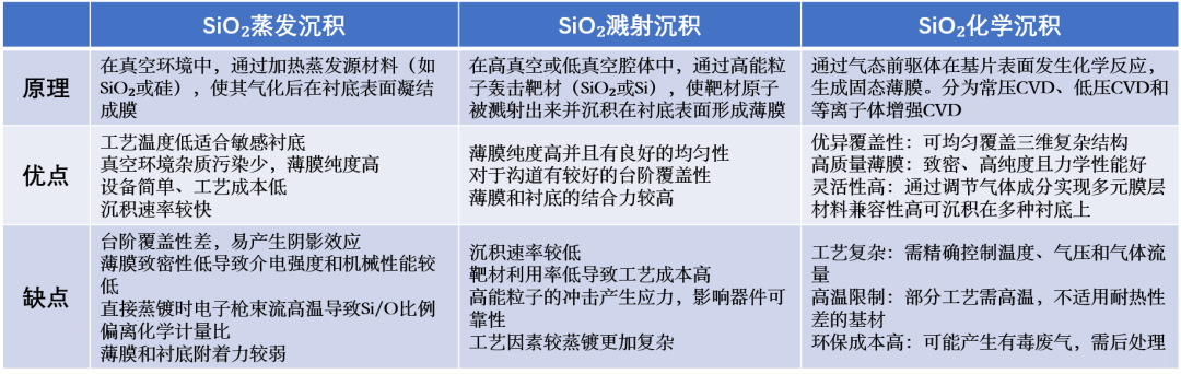
Figure 24: Comparison of Three Film Processes for Growing SiO₂
The Micro Sculptor – Etching Process
Michelangelo said that sculpture is about releasing the image trapped in marble. In the life spectrum of Surface Acoustic Wave (SAW) filters, if photolithography is the poet defining the soul, and thin film growth is the craftsman forging the body, then the etching process is the micro sculptor that gives it form. The etching process transfers the design patterns under the photoresist mask onto the wafer through ion beam etching or reactive ion etching, with the core difference from thin film processes being that thin films add material, while etching removes it.
Etching technology is mainly divided into dry etching and wet etching.Dry etching relies on the synergistic effect of high-energy ions in plasma and chemical reactions, achieving anisotropic etching with nanometer-level precision by adjusting gas composition and process parameters, particularly suitable for processing vertical structures and high aspect ratio patterns. Dry etching equipment is usually complex and expensive, and ion bombardment may cause lattice damage to the material, requiring fine tuning for compatibility with multilayer heterogeneous materials. In contrast, wet etching uses acidic, alkaline, or oxidizing solutions to chemically react with materials to dissolve and remove them, offering low cost, high efficiency, and suitability for large-area uniform processing, commonly used for photoresist stripping, wafer cleaning, and other non-critical process steps. However, its isotropic etching characteristics lead to severe lateral etching, making it difficult to meet precision requirements for linewidths below a micron, and the treatment of chemical waste also poses environmental challenges. From the metal layers of filters to three-dimensional stacked chips, from MEMS sensors to quantum devices, the continuous evolution of etching technology will become the core driving force for breaking physical limits and empowering the next generation of microelectronics manufacturing.
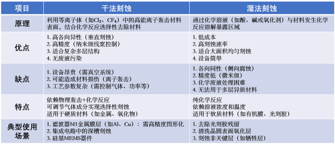
Figure 25: Comparison of Dry Etching and Wet Etching
From the perspective of etching mechanisms, dry etching can be divided into three main categories:
The first category is physical etching (sputter etching): This involves the physical bombardment of the material surface by high-energy inert gas ions (such as Ar⁺), directly sputtering away atoms. Its advantage is strong anisotropy, but it has poor selectivity, low rate, and can damage the substrate, making it suitable for micro-machining of refractory metals or special materials.
The second category is chemical etching (plasma etching): This relies on active free radicals (such as F⁺, Cl⁻) in the plasma to undergo pure chemical reactions with the material, generating volatile products without ion bombardment. Its core characteristics are high selectivity and complete isotropy, but it cannot control pattern precision, mainly used for overall photoresist removal, backside cleaning, or uniform etching of dielectric layers.
The third category is physical-chemical etching (Reactive Ion Etching, RIE): This combines ion bombardment and chemical reactions, where ions weaken the material’s bond energy, and free radicals accelerate the reaction to generate volatile products. By adjusting parameters, it can balance high anisotropy and high selectivity, supporting precise etching of complex patterns, accounting for over 90% of modern semiconductor dry etching applications, and is the core technology for advanced processes of ≤7nm.
From the perspective of equipment/plasma source, dry etching can be further divided into ICP etchers (Inductively Coupled Plasma) and CCP etchers (Capacitively Coupled Plasma), both of which ionize process gases using RF energy to generate plasma containing ions, electrons, and active free radicals to assist in etching. ICP etchers have a reaction chamber surrounded by a helical coil (or planar coil) at the top or side, connected to an independent RF power supply, while the sample stage is connected to another independent RF bias power supply. Energy is transferred through magnetic fields to induce electric fields, resulting in highly concentrated plasma in the central region of the chamber with extremely high density. CCP etchers primarily transfer energy through high-frequency electric fields to directly accelerate electrons, with plasma concentrated near the electrodes (especially on the powered electrode side) and lower density. The key advantage of ICP over CCP lies in its decoupled control capability, allowing for independent and broader adjustment of chemical activity (free radical concentration/flux) and physical bombardment intensity (ion energy). This gives ICP a significant advantage in achieving high-performance, complex RIE (mixed etching), especially in scenarios requiring high aspect ratios and precise profile control. CCP/ICP can also achieve biased chemical etching: by operating in low bias or no bias modes, physical bombardment is suppressed, primarily utilizing active free radicals in the plasma for etching, where the etching mechanism leans more towards chemical. However, pure physical etching (such as sputter etching) usually requires specialized equipment (such as IBE).
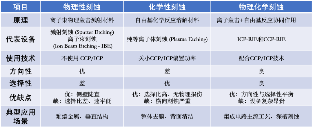
Figure 26: Main Classifications of Dry Etching
In the SAW process, two types of dry etching are mainly used: 1. ICP-RIE etching, which achieves high-precision etching of Al/Cu alloy metal layers using gas mixtures such as Cl₂/BCl₃/Ar to form the required IDT structure. As mentioned earlier, the IDT precision morphology formed by this method is generally better than that of the Lift-off process; 2. ICP/CCP chemical etching, using CF₄/O₂/CHF₃ as the main components to etch the passivation layer, achieving the effect of opening pad windows, although this etching has lower precision.
The Nano Beautician – Trim Frequency
As mentioned earlier, slight disturbances in IDT linewidth and film thickness can lead to frequency fluctuations. Taking the B25 duplexer as an example, since the isolation frequency band between the TX and RX of the device is only 15MHz, to balance insertion loss and isolation, the actual production margin is often only around ±2MHz, which is extremely difficult to achieve with conventional process levels. At this point, Trim technology is needed to reduce production ppm and achieve high yield in mass production. Trim acts like a nano beautician with a carving knife, focusing laser precision on the chip to perform micro-surgery, correcting the “innate flaws” in frequency by minute differences.
There are three main methods for Trim processes: 1. Ion Beam Figuring (IBF), 2. Reactive Ion Beam Figuring (RIBF), 3. Mass Load Figuring (MLF). The first two are subtractive, while the third is additive. The resonant frequency of SAW devices is highly sensitive to the mass of the electrode area; increasing or decreasing the electrode mass affects the propagation speed of surface acoustic waves, with an increase leading to a decrease in resonant frequency and a decrease leading to an increase. By precisely adding or removing material on the IDT, the goal is to control the frequency on a shot basis, ultimately achieving consistent frequencies across a wafer.
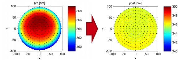
Figure 27: Comparison of Wafer Flatness Before and After Trim (Image Source: Internet)
Ion Beam Figuring Technology (IBF) is a precision surface processing method based on the physical sputtering effect, where a high-energy ion beam (such as argon ions) generated by an ion source bombards the workpiece surface, causing atomic-level “cascade collisions” to achieve non-contact material removal. This process involves momentum exchange, which may lead to subsurface damage, with the extent of damage positively correlated with ion beam energy.
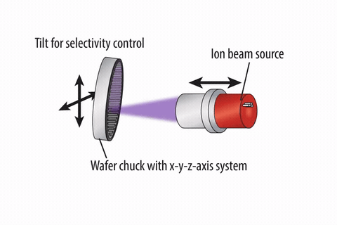
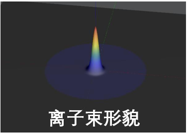
Figure 28: IBF Diagram (Image Source: Internet)
Reactive Ion Beam Figuring Technology (RIBF) combines physical sputtering and chemical reactions. Depending on the type of material being etched, a specific chemical gas or gas mixture is selected and introduced into the ion source discharge chamber to ionize and form various ions, which are then extracted into a beam for processing. The reactive gas ions physically bombard the material while simultaneously chemically reacting with the atoms being struck. The physical bombardment sputtering gives the workpiece surface atoms energy, raising the material’s surface temperature and accelerating the chemical reaction process; the chemical reaction alters the surface characteristics of the workpiece material, enhancing the physical sputtering process, thus forming an ion-enhanced reaction. The volatile products generated during processing are quickly removed by the vacuum system, allowing reactive ion beam processing to develop deeper. The core advantage is low-temperature processing, reducing impact on the subsurface, and achieving high selectivity.
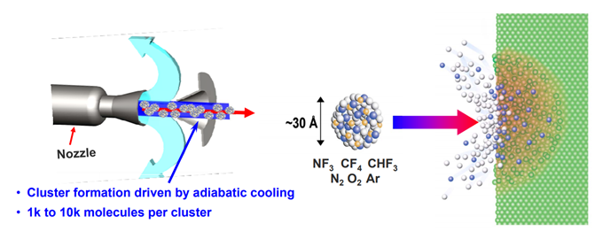
Figure 29: RIBF Diagram (Image Source: Internet)
Mass Load Figuring (MLF) involves depositing a thin layer of aluminum oxide film on existing metal electrodes (such as aluminum) through physical vapor deposition. The density of aluminum oxide is typically higher than that of aluminum, thus increasing the mass of the electrode area. The deposited aluminum oxide is an insulator, and if deposited on the metal electrode, it will not significantly change the resistivity of the metal electrode itself. If the deposition process or material affects the microstructure of the metal electrode or forms a thin interface layer, it may slightly increase resistance, and this aluminum oxide cover layer will also affect the propagation characteristics of sound waves at the edges of the electrode.
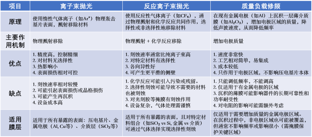
Figure 30: Comparison of Three Trim Devices
When selecting frequency trimming technology, it is essential to consider the direction of frequency adjustment, precision requirements, efficiency, cost, material impact, and the final performance requirements of the device. However, in practice, the core of Trim is often not the equipment but the algorithm. An advanced frequency trimming algorithm can yield unexpected results, as shown in Figure 31, where the frequency concentration achieved with the Trim device combined with self-developed algorithms shows significant improvement. This is also the key to achieving high yield in mass production of high roll-off devices like the B25 duplexer and B25+66 quadruplexer. It is worth noting that the role of Trim devices is not limited to this; they can also be used in various processes for fine-tuning the uniformity of thin film materials. For example, in some sputtering TC-SAW processes, to avoid the challenges of controlling CMP process precision, a more precise and simpler Trim process is chosen to refine the thickness of the SiO₂ layer, albeit with lower efficiency and higher costs.
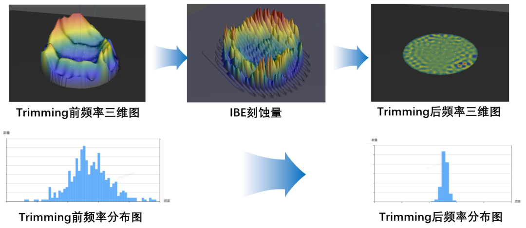
Figure 31: Schematic of the SAW Frequency Trimming Process (Some images sourced from the internet)
Thus, using the simplest Normal-SAW as an example, we have introduced the common process types in the SAW wafer fabrication process. However, the family of acoustic wave filters has other branches; what clever features do they possess, what surprises do they bring us, and how should we choose? Stay tuned for the next issue,To Be Continued…