Source: APEC2024-(Wolfspeed)Author: Dereje Woldegiorgis, PhD
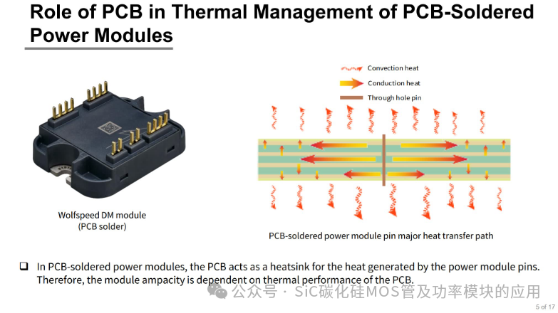
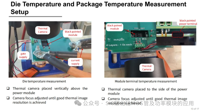
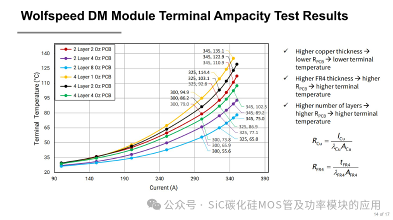
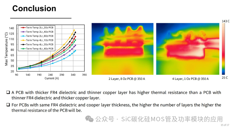
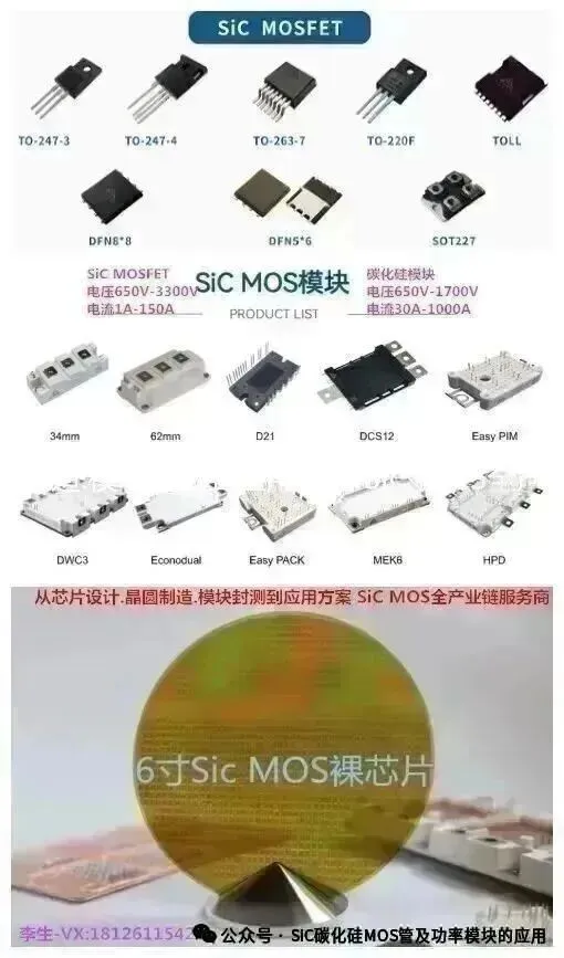
 Note: The images in the report are unrelated to the text.
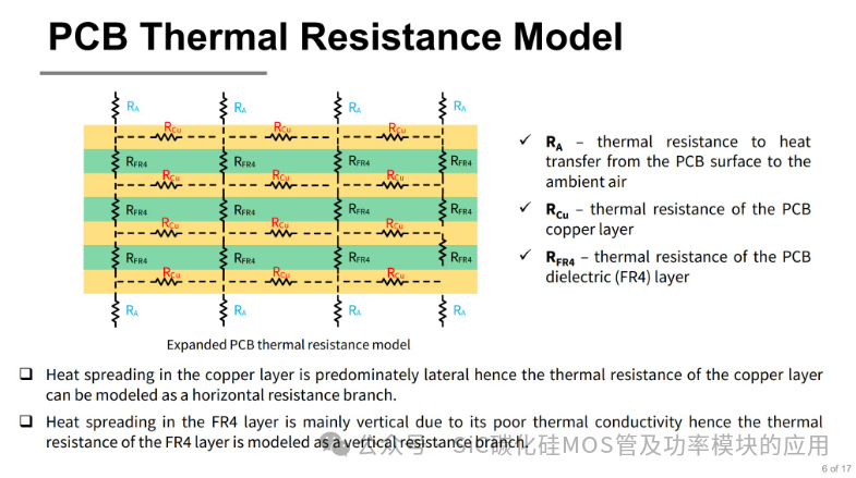
The design of the PCB has acrucial and even decisive impact on the current carrying capacity of silicon carbide power modules. Silicon carbide devices have advantages such as high power density, high switching frequency, and high operating temperature, but if the PCB design is inadequate, these advantages cannot be realized and may even lead to system failure.
In simple terms,poor PCB design can become a bottleneck for the entire power circuit, limiting current carrying capacity and causing overheating, voltage overshoot, electromagnetic interference, and a series of other issues.
Here are several key aspects of PCB design that affect current carrying capacity:
1. Conduction Current Capacity
This is the most direct impact, mainly depending on thecross-sectional area of the PCB traces and thetemperature rise.
Trace Width and Thickness:
The principle: According to the current formula
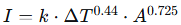
(where I is the current, ΔT is the temperature rise, A is the cross-sectional area), the current carrying capacity is directly related to the trace cross-sectional area.
Design Points:
Sufficient Width: The traces in the power circuit (especially the main current path) must be wide enough. PCB current carrying capacity calculation tools (such as IPC-2152 standard) should be used to determine the minimum trace width.
Increase Copper Thickness: Using thicker copper foil (such as 2oz/70μm, or even 3oz/105μm) can significantly increase current carrying capacity without excessively increasing board area. This is a common practice in high current applications.
Remove Solder Mask: Opening windows (removing solder mask) on traces that require high current and plating with thick tin can further increase effective cross-sectional area and heat dissipation capacity.
Via Treatment:
Issue: When current needs to switch layers, vias become a bottleneck. The current carrying capacity of a single via is limited (usually 1A-3A, depending on size and plating process).
Design Points:
Multiple Vias in Parallel: For high current paths, via arrays (multiple vias in parallel) must be used to share the current. A rule of thumb is to use at least 1-2 standard vias for every ampere of current.
Increase Via Size: Larger diameter vias have lower resistance and higher current carrying capacity.
Fill with Conductive Epoxy: For extreme current applications, via filling processes can be used to further reduce resistance and improve heat dissipation.
2. Thermal Management Capability
Current carrying capacity is essentially temperature limited. The PCB is one of the main paths for heat dissipation in power modules. Poor thermal design can lead to localized overheating, and even if the traces can theoretically handle the current, the module may derate or fail due to high temperatures.
Heat Dissipation Vias:
Function: Place a dense array of heat dissipation vias directly under the heat sink pads of power devices (such as SiC MOSFETs). These vias quickly conduct heat from the top layer to the inner or bottom copper planes, thereby expanding the heat dissipation area.
Design Points: Vias should be as small and numerous as possible, and filled with thermal conductive epoxy for optimal effect.
Internal Copper Planes:
Function: Use complete inner layers (power or ground layers) as heat dissipation layers. These large copper layers are excellent heat spreaders, capable of evenly distributing hotspot heat across the entire PCB or conducting it to external heat sinks.
External Heat Dissipation Path:
Function: Ensure that high heat-generating areas on the PCB (such as power module locations) are in close contact with metal housings or external heat sinks through thermal pads. The PCB layout needs to allow space and screw holes for heat sink installation.
3. Impact of Parasitic Parameters (“Effective” Current Carrying Capacity under High Frequency Switching)
This is aunique and critical challenge in silicon carbide applications. The switching speed of SiC is extremely fast (in the ns range), making the parasitic inductance introduced by PCB layoutextremely detrimental.
Hazards of Parasitic Inductance:
Voltage Overshoot and Ringing: Loop parasitic inductance Lloop interacts with the high-speed di/dt of the switching device, generating significant voltage overshoot Vovershoot=Lloop⋅di/dt. This may exceed the rated voltage of SiC devices, leading to damage.
Increased Switching Losses: Parasitic inductance prolongs switching times, increases switching losses, and raises the junction temperature of the device. This means that under the same average current, the actual thermal stress is greater, thus limiting the “effective” current carrying capacity.
Electromagnetic Interference: Severe voltage ringing can generate strong electromagnetic interference.
Optimize Layout to Minimize Parasitic Inductance:
Compact Layout: The physical area of the core power loop (e.g., DC+ → decoupling capacitor → SiC module → DC-) must beminimized. This means that related components should be placed close together.
Implement “Stacked” Structure: The ideal approach is to use multilayer boards, arranging the positive and negative paths of the power loop on adjacent layers and closely overlapping. This parallel plate structure can create natural field cancellation, significantly reducing loop inductance.
Use Low ESL Capacitors: Decoupling capacitors should be selected from types designed for high frequency (such as ceramic capacitors) and placed directly near the pins of the power module, with pins kept as short and wide as possible.
Conclusion: Key Principles of Excellent PCB Design
To maximize the current carrying capacity and reliability of SiC power modules, PCB design should adhere to the following principles:
| Design Goals | Specific Measures |
|---|---|
| Reduce DC Resistance | 1. Widen power traces.2. Increase copper foil thickness.3. Use via arrays for current layer switching.4. Large current traces should be windowed and tin-plated. |
| Optimize Heat Dissipation | 1. Design heat dissipation via arrays under the devices.2. Use large internal copper planes as heat dissipation layers.3. Plan the path to external heat sinks. |
| Minimize Parasitic Inductance | 1. Extremely compact power loop layout.2. Use stacked bus design (adjacent layers overlapping).3. High frequency decoupling capacitors placed close to device pins. |
| Ensure Mechanical Reliability | Avoid sharp right angles and acute angles on power traces; use arcs or 45° angles to reduce current crowding effects (similar to antenna effects) and thermal stress concentration. |
Conclusion:
In silicon carbide power module applications, the PCB is no longer just a simple electrical connection carrier; it is itself acritical power and thermal management component. A well-optimized PCB design can ensure that the immense potential of SiC devices is safely and efficiently unleashed, achieving higher power density, greater efficiency, and smaller system size. Conversely, a poor PCB design can become an insurmountable bottleneck, leading to decreased system performance or even failure.
Note: This article is sourced from the internet for the purpose of sharing more information. The views expressed in the article are for sharing and communication only and do not represent the position of this public account. Please indicate the source when reprinting. If there are any errors in source attribution or copyright issues, please contact us, and we will promptly correct or delete them. Thank you. Focused on the research and application of silicon carbide devices. Sharing industry materials related to the design, research and development, and application of silicon carbide devices.To join the communication WeChat group, please add personal WeChat: 18126115420, and note your company + name + research direction.