1
Introduction
This article summarizes the hardware design experience based on a certain Bluetooth module and is intended for hardware design reference only.
2
Antenna Design
2.1 PIFA Antenna Design
2.1.1 Size Requirements
The size of this antenna is derived from theoretical calculations based on frequency characteristics and has been validated through practical design experience, which is related to the substrate material and environment. If designed according to the following specifications, the maximum unobstructed distance can reach 20 meters.
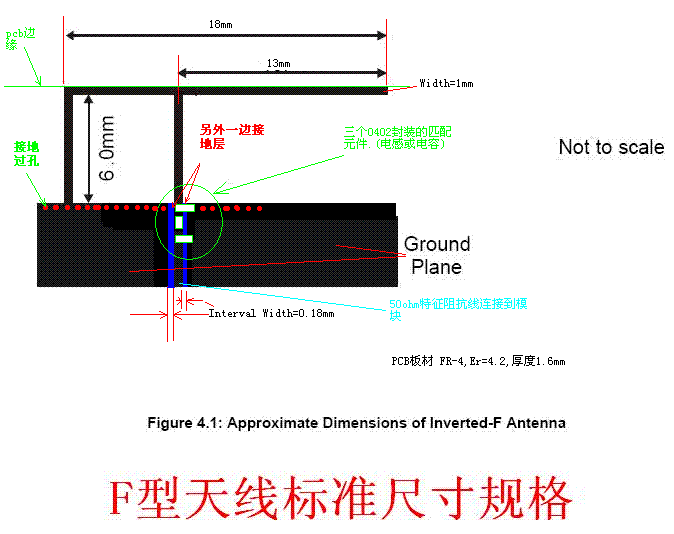
Figure 1
2.1.2 Wiring Requirements
First, it is recommended to design the antenna as a component package according to size for easy placement and subsequent project design, which can prevent size changes caused by movement and avoid repeated modifications.
Secondly, this antenna is connected to the ground line, and no components or wiring should be placed around the effective part of the antenna and its lower layer (the back side), nor should copper be laid, otherwise it will affect signal transmission and reception, or even prevent normal operation.
Third, the grounding point of this antenna requires a large area of grounding and multiple holes should be punched.
Fourth, the antenna should be designed at the edge of the PCB board, preferably facing the front panel, and surrounding iron structures should be avoided. 2.1.3 Substrate Requirements
Please use FR4 as the substrate material with a dielectric constant of 4.2. 2.2 External Antenna Design
Please disconnect the connection circuit of the PIFA antenna and connect the external antenna with a 10pF capacitor. The external antenna’s wiring should use a 50-ohm high-frequency shielded cable, and 3CM of the shielding layer should be removed from the end. The center signal wire at the end should be soldered to the antenna output terminal, and the shielding wire should also be soldered to a nearby ground position. The tail of the antenna should be placed in the front panel’s forward position or lead outside the metal shell.
3
Power Supply Design
The parameter requirements for the power supply should be designed based on the specific model’s parameters. Please refer to the corresponding model’s SPEC document for details.
Note: To ensure the stability of the module’s operation and to avoid interference with voice output, it is recommended that the Bluetooth module be powered by an independent power supply, ensuring power stability and that the output power meets the module’s maximum power consumption.
Additionally, during power loss, ensure that the Bluetooth module is completely powered off (i.e., ensure that the power-off voltage can be less than 1.5V for over 50mS); if this condition cannot be met, please add a reset chip to control the reset level of the module’s reset pin.
Recommendation: The main control CPU should add power control for the Bluetooth module, which can ensure complete power-off of the module and avoid inconsistencies between the Bluetooth module’s status and the CPU’s status.
4
Audio Circuit Design
The design of the audio circuit directly affects the audio quality indicators output by the Bluetooth module; therefore, it should be independently differentiated in wiring to ensure the integrity of the audio signal. 4.1 Differential Output Design Requirements
Some modules output audio as differential signals, requiring an external differential-to-single-ended signal conversion circuit. As shown in the figure below:
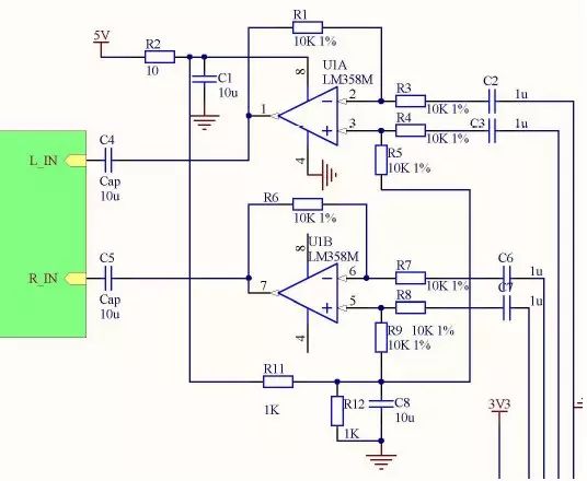
Figure 2
The routing of the differential lines should be as short and equal in length as possible, with proper grounding shielding to avoid interference with the signal lines.
Secondly, its grounding network should connect to the audio ground of the target system (e.g., the amplifier grounding point of a car audio system) before connecting to the ground to avoid introducing interference through the ground line.
Third, it is recommended that all 10K resistors in the diagram use 1% precision. Fourth, ensure the stability of the power supply voltage. 4.2 Stereo Single-Ended Output Design Requirements
All modules with built-in audio conversion circuits output stereo single-ended signals. In its design, care should be taken to avoid audio output wiring near high-power components and high-frequency signal lines; additionally, ensure the integrity of the audio ground, i.e., the AGND signal should connect to the audio ground of the target system (e.g., the amplifier grounding point of a car audio system) before connecting to the ground to avoid introducing interference through the ground line.
5
MIC Circuit Design
5. MIC Circuit Design5.1 Module MIC Design Requirements
Some modules do not have a built-in microphone input voltage bias circuit and require an external voltage bias circuit to ensure the MIC operates normally and stably, as shown in the figure below:
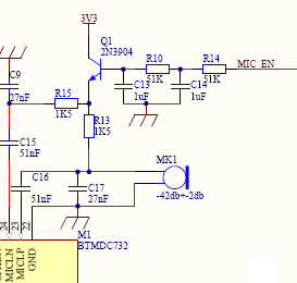
Figure 3
Here, MIC_EN is the voltage signal output control from the module’s PIO11. Additionally, the following points should be noted: First, for the MIC specifications, please choose an omnidirectional MIC with a specification of -42dB (±3dB);
Secondly, the MIC circuit should have independent wiring, especially the MICGND should connect to the corresponding pin of the module, and it is prohibited to connect to the system ground for convenience before connecting to the module’s ground—this is to prevent interference with the MIC input.
Third, the diameter of the panel hole for the MIC should be determined according to the size of the MIC; otherwise, it will cause attenuation of the MIC input signal, affecting its sensitivity;
Fourth, the MIC should be fitted with a rubber gasket and directly pressed tightly against the machine’s panel to prevent interference from vibration.5.2 Other Module MIC Design Requirements
Additionally, some modules have built-in microphone input voltage bias circuits, so the hardware design only needs to connect the MIC’s P/N pins to the corresponding MIC input P/N pins of the module to work normally. Design considerations can refer to section 5.1.
For more technical content, please click “Read the original text”.

RFsister Edited and Organized
Reprint Statement: This article aims to provide industry news reading for the RF technology community. If there are any inaccuracies or infringement issues, please contact us for processing! Respect knowledge, respect originality!
Submission Email: [email protected]