PCB Design Basics: The Relationship Between Trace Width and Current

In the process of PCB design, many beginners may wonder: how wide should this trace be? Why are power lines much thicker than signal lines? Today, we will discuss the important relationship between PCB trace width and current. Why is Trace Width Important? The traces on a PCB are equivalent to “wires” in a circuit. … Read more

Understanding the Impact of PCB Design on the Current Carrying Capacity of Silicon Carbide (SiC) Power Modules

Understanding the Impact of PCB Design on the Current Carrying Capacity of Silicon Carbide (SiC) Power Modules

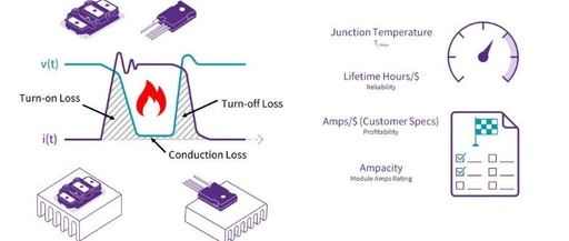
Source: APEC2024-(Wolfspeed)Author: Dereje Woldegiorgis, PhDNote: The images in the report are unrelated to the text. The design of the PCB has acrucial and even decisive impact on the current carrying capacity of silicon carbide power modules. Silicon carbide devices have advantages such as high power density, high switching frequency, and high operating temperature, but if … Read more

PCB Trace Width and Current Relationship: Calculation and Reference

PCB Trace Width and Current Relationship: Calculation and Reference

1. The calculation method is as follows: First, calculate the cross-sectional area of the track. Most PCB copper foil thickness is 35um (if unsure, you can ask the PCB manufacturer; 1 ounce is 35um, but it is often less than 35um). The cross-sectional area is obtained by multiplying the trace width by the thickness, and … Read more

How PCB Boards Can Withstand Over 100A Current

How PCB Boards Can Withstand Over 100A Current

Typically, the current design for PCBs does not exceed 10A, especially in home and consumer electronics, where the continuous working current on a PCB usually does not exceed 2A.However, some product designs for power traces can sustain continuous currents of around 80A. Considering instantaneous currents and leaving a margin for the entire system, the continuous … Read more

Key Points and Standards for Power PCB Design (Systematic Compilation)

Key Points and Standards for Power PCB Design (Systematic Compilation)

1. Power Connector Design Standards Electrical Clearance and Creepage Distance The electrical clearance between the power and protective ground (PGND) should be ≥2mm, and the creepage distance should be ≥2mm (before the fuse) or ≥1.4mm (after the fuse). The distance between PGND and other signals (such as GND, low-speed signals) should be ≥2mm, and the … Read more

Current Carrying Capacity of PCB Traces and Vias

Current Carrying Capacity of PCB Traces and Vias

Introduction The electrical connections between various components on FR4 copper-clad PCBA are achieved through the copper foil traces and vias on its layers. Due to the varying current levels in different products and modules, designers need to know whether the designed traces and vias can carry the corresponding current to fulfill the product’s functionality and … Read more