1 SoC Concept
System on Chip vs. System on PCB: The essence is to evolve the process technology to transform a module into an internal module.
-
SoC aims for high integration and miniaturization within a single chip. SoC serves as the core, and it is certainly expanded and connected through PCB.
-
System on PCB seeks flexibility and functional expansion through discrete components at the circuit board level.
In-depth Comparison: SoC vs. System on PCB
| Feature | System on PCB (SoPCB) | System on Chip (SoC) |
| Core Idea | Discrete Integration | Monolithic Integration |
| Composition | Multiple independent functional chips (CPU, memory, PHY, ADC, etc.) connected via PCB traces. | Integration of CPU, GPU, memory controller, DSP, various peripheral interfaces, etc., into a single chip. |
| Advantages | 1. Design flexibility: Ability to choose the best components from different manufacturers.2. Easy debugging and maintenance: Faulty chips can be measured and replaced individually.3. Short development cycle: Relatively low cost, suitable for prototype validation and small batch production. | 1. Extremely small size: Greatly saves space, suitable for portable devices like phones and watches.2. Low power consumption: Internal interconnect power consumption is much lower than board-level interconnects.3. High performance: On-chip bus speed is much higher than board-level bus, with lower latency.4. Low cost in mass production: Although chip design costs are high, the cost per chip in mass production is lower than purchasing a bunch of discrete chips. |
| Disadvantages | 1. Larger physical size.2. Relatively higher power consumption (signals travel longer distances on PCB, with larger parasitic capacitance/inductance).3. Greater signal integrity challenges (high-speed signals are prone to interference).4. High cost for mass production (requires procurement and soldering of numerous discrete components). | 1. Extremely complex design and manufacturing, with a high barrier to entry (typically the domain of giants like Apple, Qualcomm, HiSilicon, etc.).2. One-time investment (NRE) costs are astronomical (tens of millions to hundreds of millions of dollars).3. Poor flexibility: Once the chip is fabricated, functionality cannot be changed.4. Difficult debugging: Internal signals of the chip are hard to probe. |
| Typical Examples | 1. Arduino, Raspberry Pi (early models): CPU, memory, and IO controllers are all independent chips.2. Desktop computer motherboards: CPU, memory modules, graphics cards, and network card chips are all independent, plugged into or soldered onto the PCB. | 1. Mobile application processors (e.g., Apple A series, Qualcomm Snapdragon, MediaTek Dimensity): integrate CPU, GPU, NPU, memory controller, image processor, etc.2. The core of Raspberry Pi CM4: its core is a Broadcom SoC.3. Modern router chips: integrate CPU, switching matrix, PHY, etc., into one. |
System on PCB is a classic method for implementing electronic systems, while SoC is the ultimate extension and high integration of this method at the chip level.
1.1 SoC Design Process – Hardware-Software Co-design Process
If a requirement is established from the beginning, how to proceed with development:
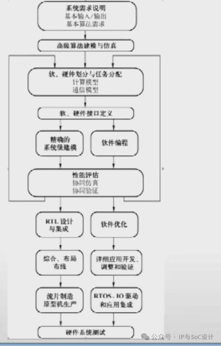
Here, the classic SoC flowchart from ARM is often used as an example:
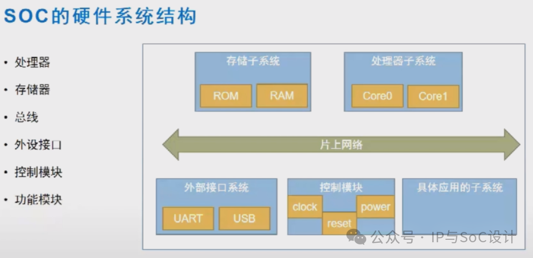
1 How Software and Hardware Interact
2 How to Divide Software and Hardware
2 CDC in SoC
CDC is a key point in SoC design; an SoC contains high-speed CPUs and high-speed peripherals; it is essential to maximize the performance of each system. Therefore, there must be different clocks; generally, a reference clock is input externally, and various high-speed clocks are generated internally by the PLL in the CRG module.
2.1 Hazards of CDC
0 Clock Domain
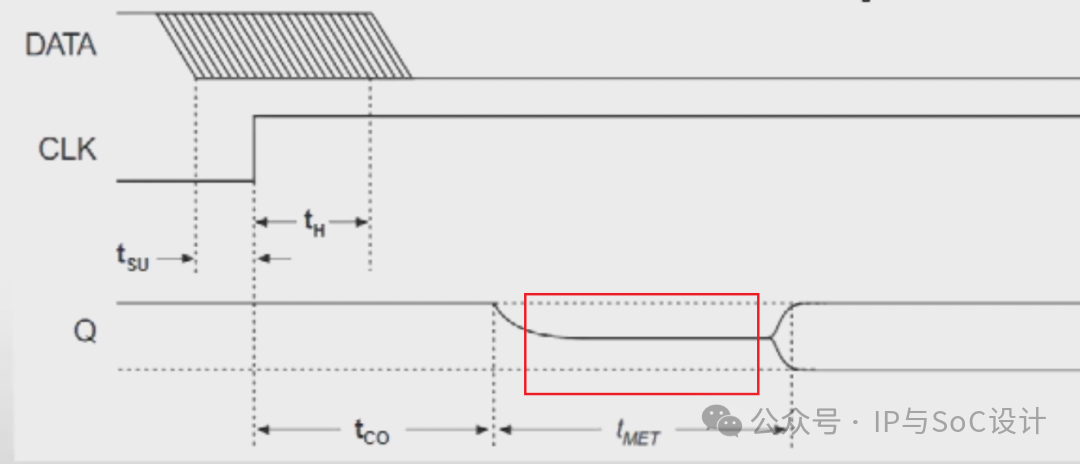
1 Metastability
Actual phenomenon: The red area indicates the unstable metastable state, which is represented as X state in simulation, with serious consequences due to oscillation and propagation; however, the benefit is that it stabilizes over time like a roller coaster, eventually becoming a stable state.
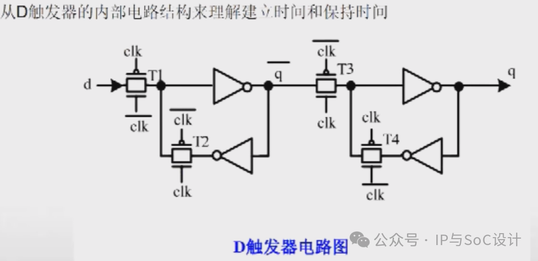
D Flip-Flop Circuit Structure:
2 Data Loss
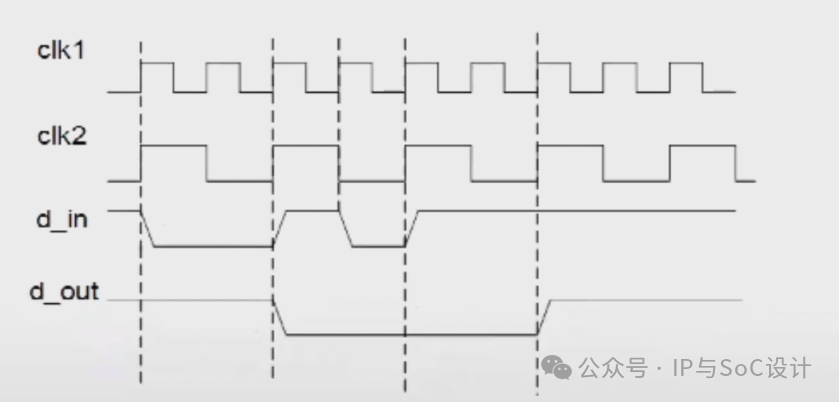
3 Data Inconsistency – Bus Type
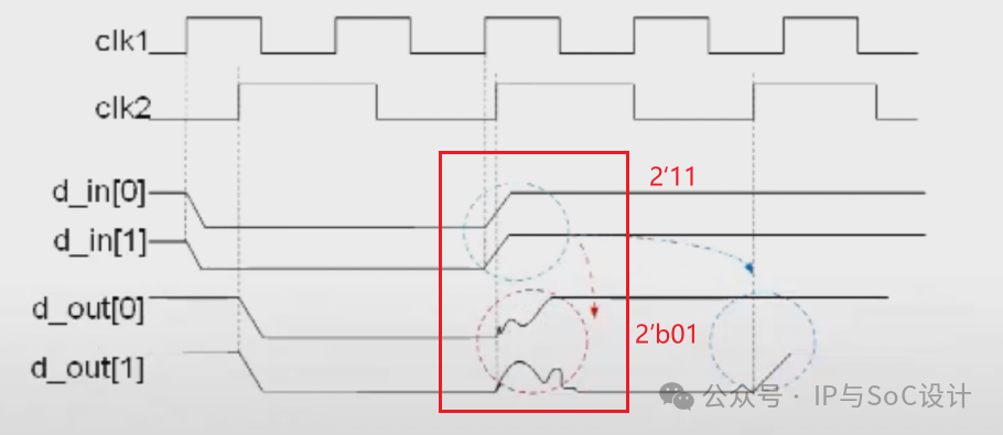
Can bus-type data signals synchronize directly for each bit?
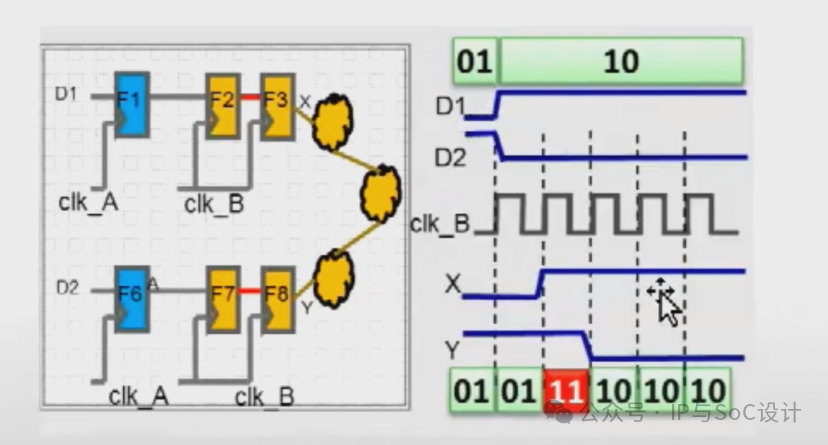
This method is not applicable for multiple bits that are related in bus-type signals; however, it can be used when multiple bits are independent.
2.2 Sync Methods and Types
1 Single Bit Level Synchronization – 2/3 Sampling
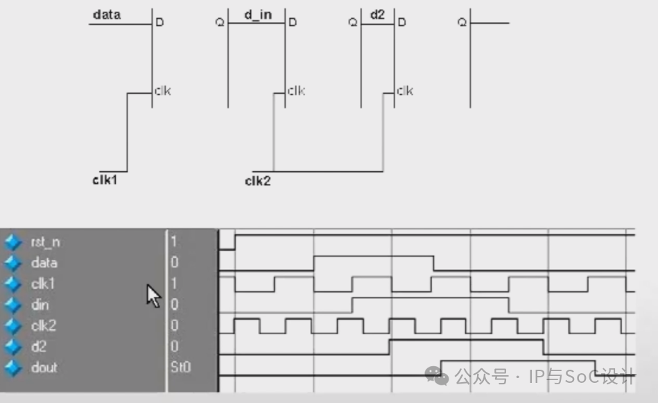
2 Edge Synchronization – 2/3 Sampling
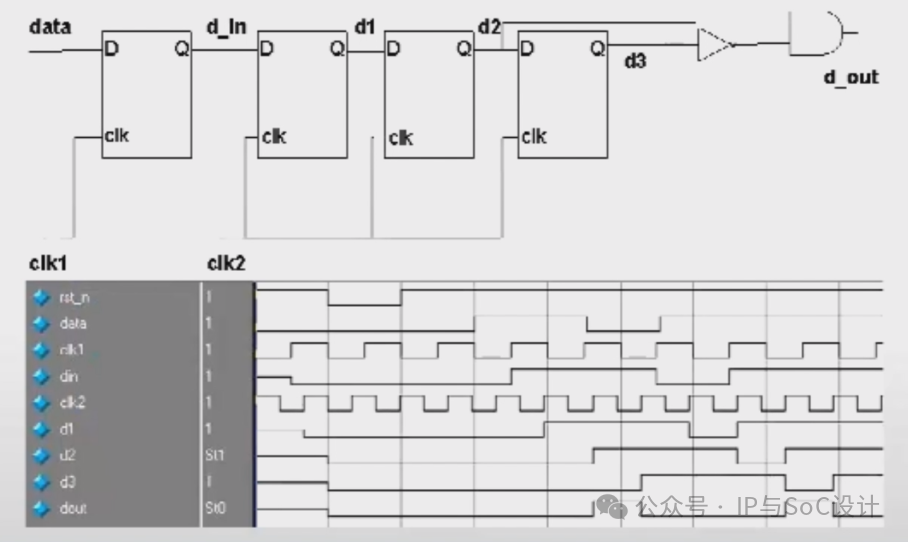
3 Pulse Synchronization – 2/3 Sampling
In the source clock domain, first widen the pulse to a level, then perform synchronization to detect the edge.
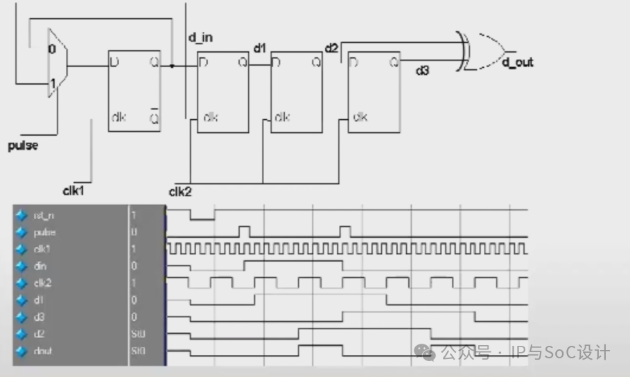
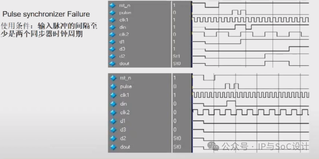
Pulse sync requirements: The interval of the input pulse must be at least the interval of two synchronizers.
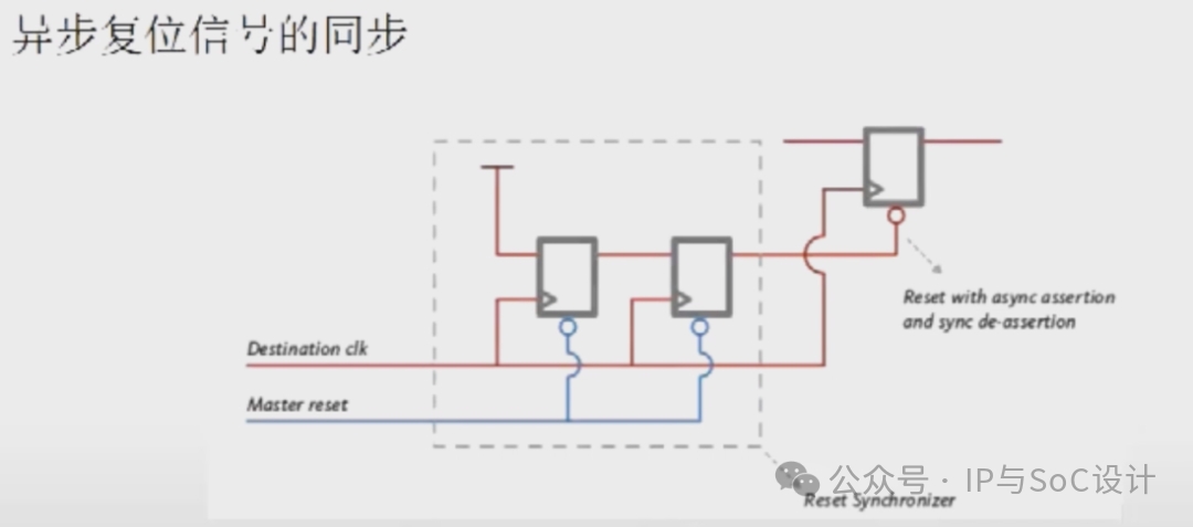
2.3 Reset Signal Synchronization
Asynchronous reset, synchronous release;
2.4 Bus-Type Data Synchronization
1 Handshake Mechanism
Here, referring to the content of the AMBA protocol makes it easy to understand.
2 Asynchronous FIFO
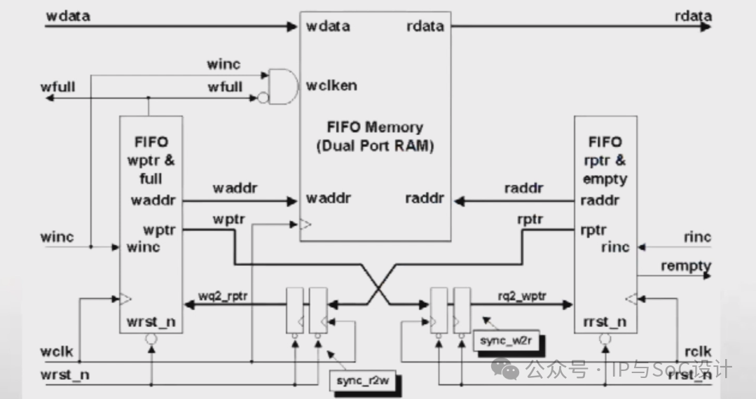
This will not be elaborated here.
3 SoC Low Power Techniques
3.1 Clock Gating
RTL and Tools
First, the designer actively adds it when writing RTL;
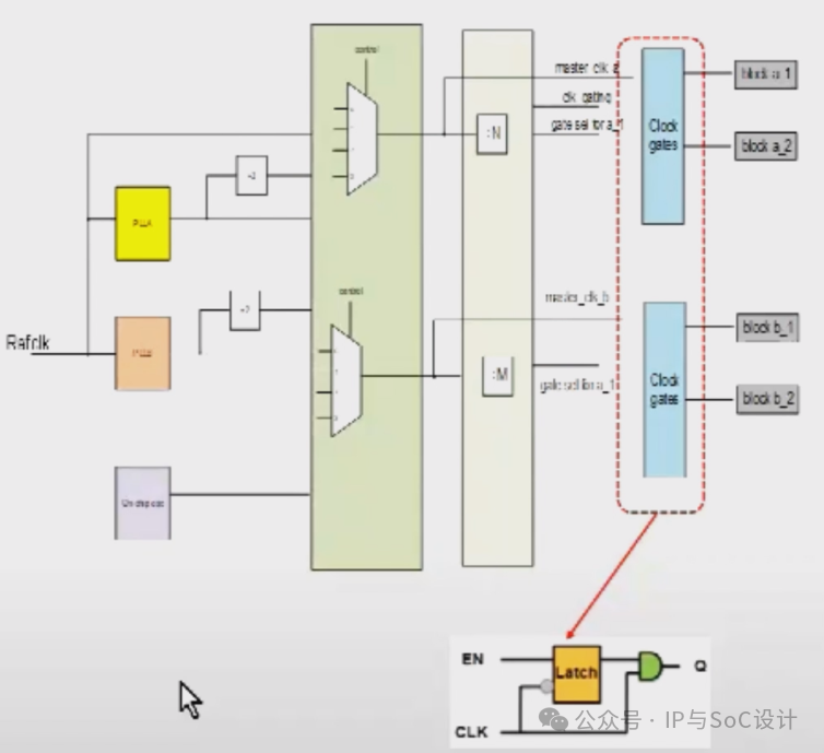
Second, tools can insert it.
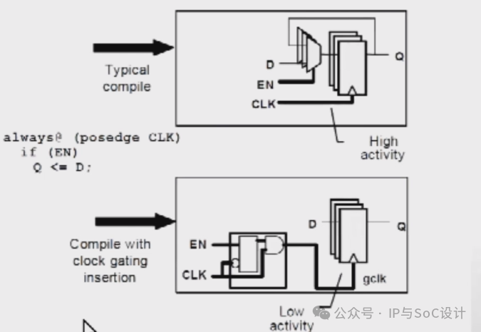
During PR, it is essential to check with the backend.
3.2 Multiple Clock Domains
3.3 DVFS – Dynamic Voltage and Frequency Scaling
Dynamic voltage switching and frequency reduction;