
-
Cut the substrate material to the required dimensions as planned before production. -
Main production material: Copper clad laminate.
-
Avoid burrs on the board edges affecting quality; after cutting, edge grinding and corner rounding should be performed. -
Consider shrinkage effects; bake the cut boards before sending them to the next process. -
Cutting must pay attention to the direction of warp and weft to ensure consistency with engineering instructions to avoid warping issues.
-
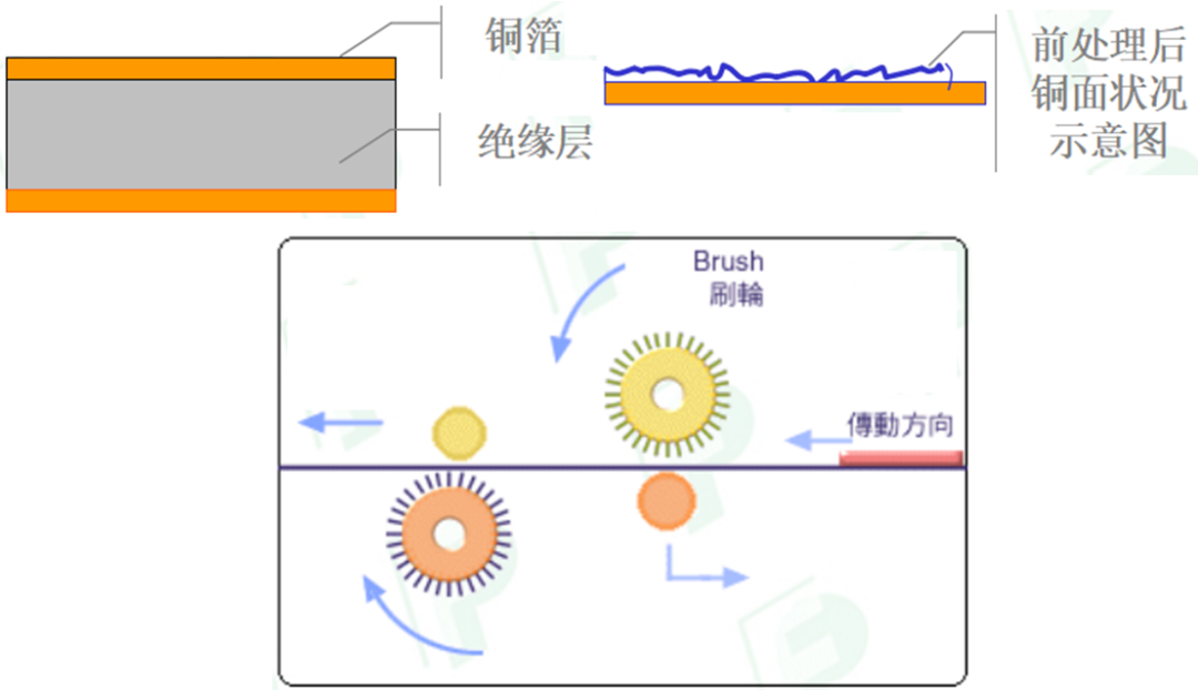
Remove contaminants from the copper surface and increase the roughness of the copper surface to facilitate the subsequent film lamination process.
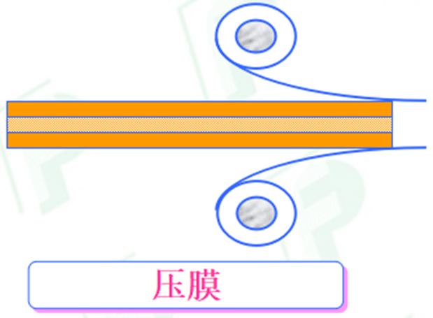
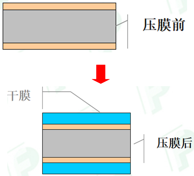
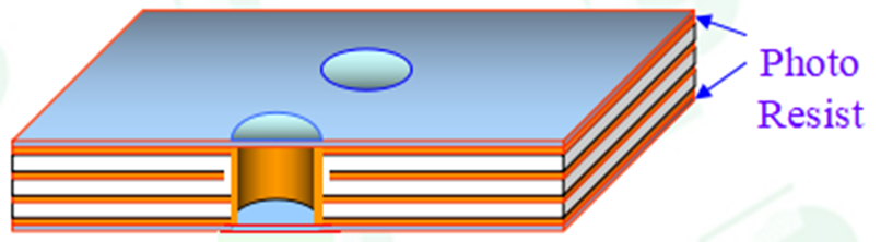
Inner Layer Circuit – Film Lamination Introduction
Film Lamination (LAMINATION):
Purpose: To apply a photoresist dry film onto the treated copper surface through heat pressing.
Main production material: Dry film.
Process principle:
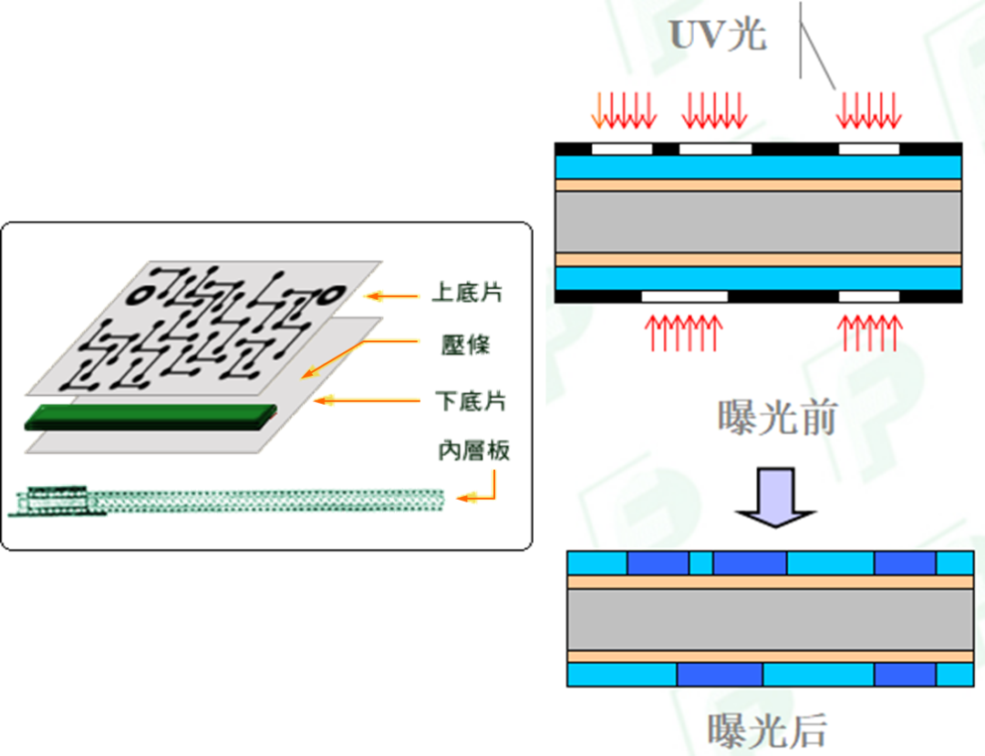
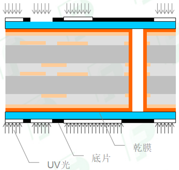
Inner Layer Circuit – Exposure Introduction
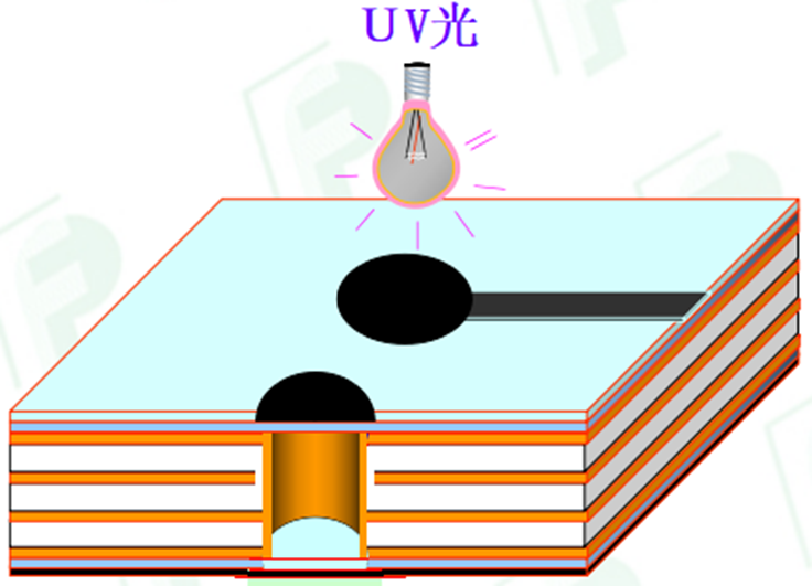
Exposure (EXPOSURE):
Purpose:
-
To transfer the image from the original film onto the photosensitive substrate through light exposure Main production tool: Film.
Process principle:
-
The white translucent parts undergo photopolymerization, while the black parts do not react due to being opaque, and during development, the areas that reacted cannot be dissolved and remain on the board surface.
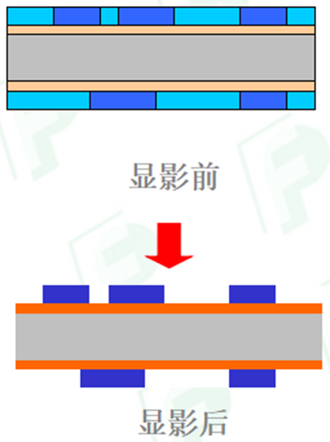
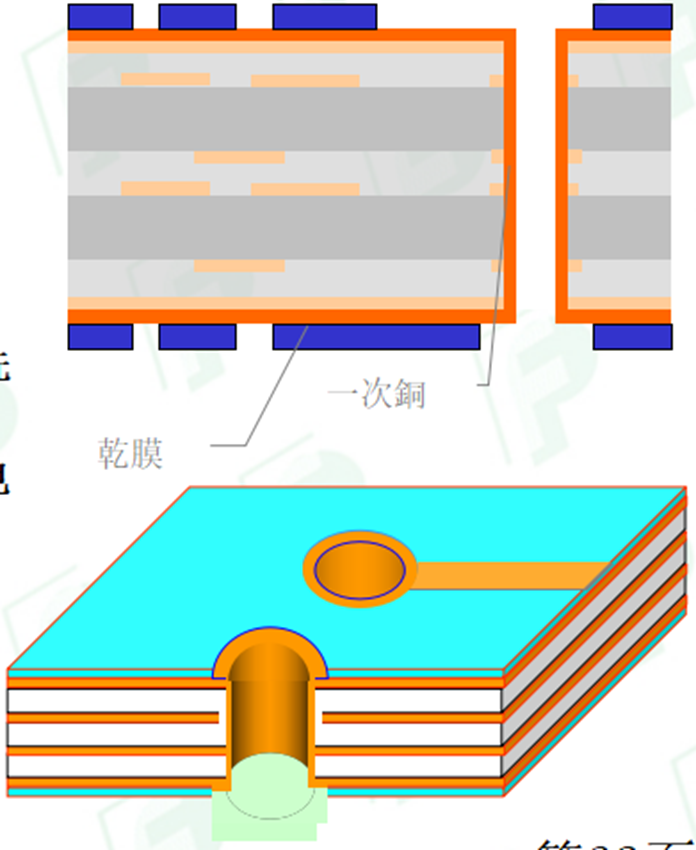
Inner Layer Circuit – Development Introduction
Development (DEVELOPING):
Purpose:
-
To wash away the undeveloped dry film portions with alkaline solution Main production material: K2CO3.
Process principle:
-
Use an alkaline solution to wash away the undeveloped dry film, while the dry film that has undergone polymerization remains on the board surface as an etching protective layer.
Note:
-
Water-soluble dry film mainly contains organic acid radicals, which react with weak bases to form salts that can be dissolved in water, exposing the pattern.
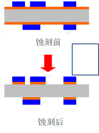
Inner Layer Circuit – Etching Introduction
Etching (ETCHING):
Purpose:
-
To use a chemical solution to etch away the exposed copper after development, forming the inner layer circuit pattern.
Main production material: Etching solution (CuCl2).
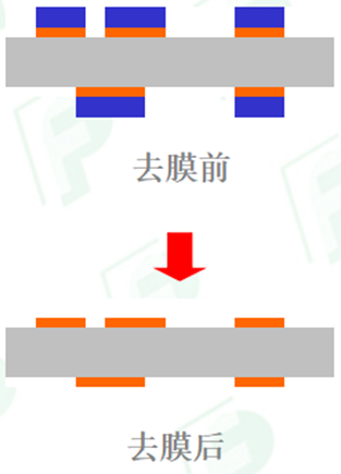
Inner Layer Circuit – Stripping Introduction
Stripping (STRIP):
Purpose:
-
To use a strong base to strip the protective etching layer from the copper surface, exposing the circuit pattern.
Main production material: NaOH.
Inner Layer Circuit – Drilling Introduction
Drilling:
Purpose:
-
To use CCD alignment to drill positioning holes and rivet holes for inspection work.
Main production material: Drill bits.
Inner Layer Inspection Process
AOI Inspection:
Full name: Automatic Optical Inspection.
Purpose:
-
To use optical reflection principles to feed images back to the equipment for processing, comparing with set logic judgment rules or data graphics to identify defect locations.
Precautions:
-
Since the testing method used by AOI is logical comparison, there will inevitably be some misjudgment defects, which need to be confirmed manually.


Process Introduction:

Purpose:
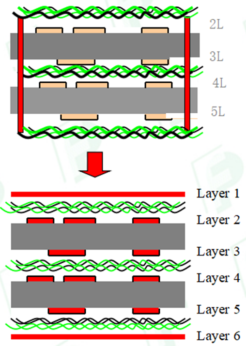
Lamination: To press copper foil (Copper), prepreg (Prepreg), and the inner layer circuit board after browning into a multilayer board.
Drilling: To drill through holes connecting the circuits between layers on the board surface.
Lamination Process – Browning Introduction
Browning:
Purpose:
(1) To roughen the copper surface, increasing contact surface area with resin.
(2) To enhance the wettability of the copper surface with flowing resin.
(3) To passivate the copper surface to avoid adverse reactions.
Main production material: Browning solution MS100.
Precautions:
-
The browning film is very thin and prone to scratching problems, so care must be taken with handling.

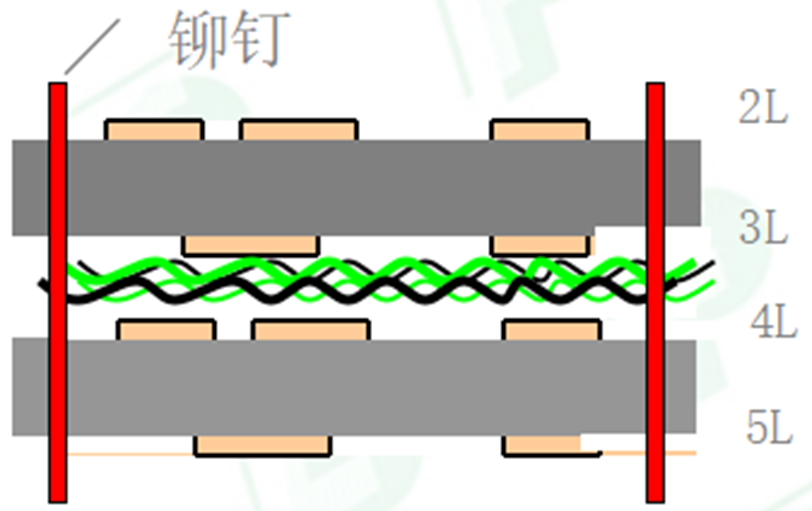
Lamination Process – Riveting Introduction
Riveting
Purpose: (Four-layer boards do not require rivets)
-
To use rivets to fasten multiple inner layer boards together to avoid interlayer shifting during subsequent processing.
Main production materials: Rivets; prepreg (P/P).
P/P (PREPREG):
Made of resin and fiberglass cloth, the types of fiberglass cloth can be divided into 106, 1080, 3313, 2116, 7628, etc.
Resins can be classified based on crosslinking status:
A stage (completely uncured); B stage (partially cured); C stage (fully cured). The P/P used in production is all in the B stage state.
Lamination Process – Stacking Introduction
Stacking:
Purpose:
-
To stack the pre-stacked boards into a form ready for pressing into multilayer boards.
Main production materials: Copper foil, prepreg.
Electroplated copper skin; categorized by thickness as follows:
1/3OZ = 12um (code T)
1/2OZ = 18um (code H)
1OZ = 35um (code 1)
2OZ = 70um (code 2)
Lamination Process – Pressing Introduction
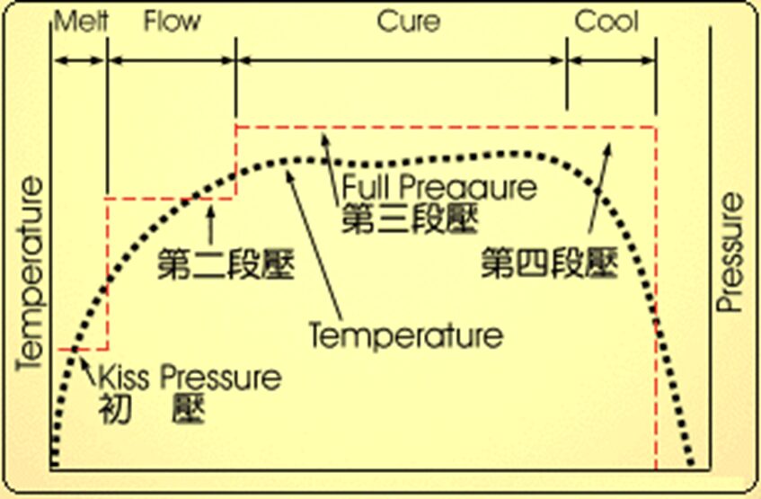
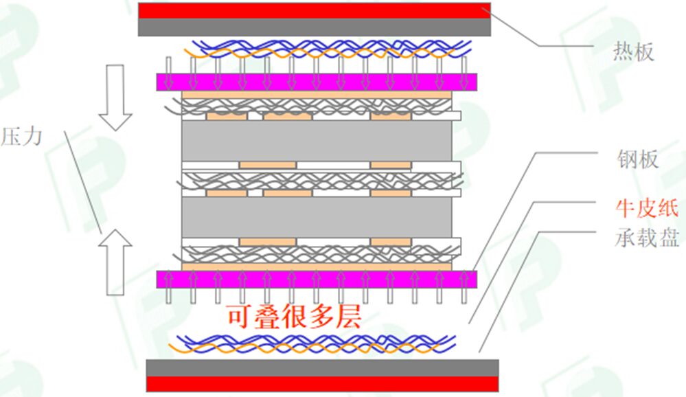
Pressing:
Purpose: To press the stacked boards into multilayer boards through heat pressing.
Main production auxiliary materials: Kraft paper, steel plates.
Lamination Process – Post-processing Introduction
Post-processing:
Purpose:
-
To perform preliminary shaping of the laminated boards through edge grinding, punching, milling, etc., to meet quality control requirements for subsequent processing and provide tool holes for later operations.
Main production materials: Drill bits; milling cutters.
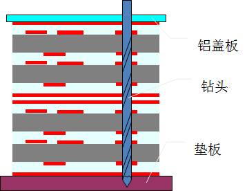
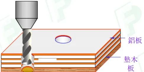
Drilling Process – Drilling Introduction
Drilling:
Purpose:
-
To drill through holes connecting the circuits between layers on the board surface.
Main raw materials: Drill bits; cover plates; backing plates.
Drill bits: Made of tungsten carbide, cobalt, and organic adhesives.
Cover plates: Mainly aluminum sheets, serving to position the drill bits, dissipate heat, reduce burrs, and prevent damage from pressure feet.
Backing plates: Mainly composite boards, serving to protect the drilling machine’s table, prevent burrs from exiting, reduce drill bit temperature, and clean drill bit grooves from glue residues.
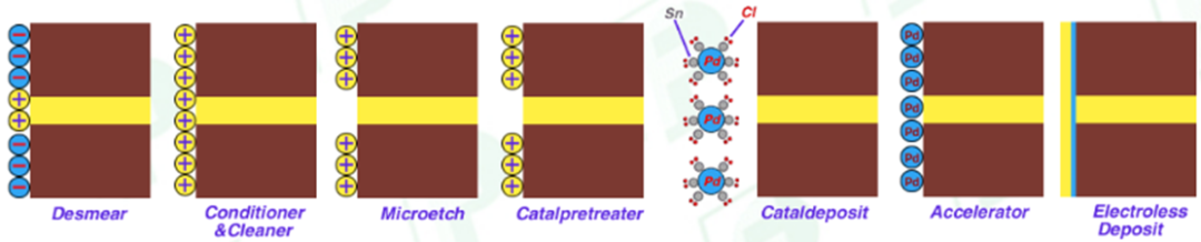
C. Introduction to Hole Metallization Process
Process Introduction
Purpose:
-
To metallize the non-conductive parts of the hole walls made of resin and fiberglass.
-
To facilitate subsequent electroplating processes, providing sufficiently conductive and protective metal hole walls.
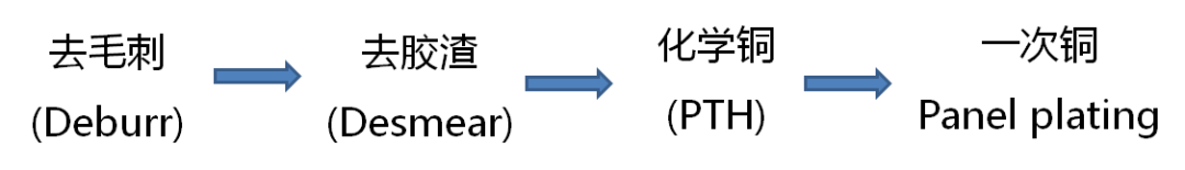
Copper Deposition Process – Deburring and Desmear Introduction
Deburring (Deburr):
Causes of burrs: Copper wires and uncut fiberglass at the edges of the holes after drilling.
Purpose of deburring: To remove burrs from the hole edges, preventing poor plating.
Main raw material: Scrubbers.
Desmear:
Causes of glue residues: High temperatures during drilling lead to glass transition temperature (Tg), causing melting and producing glue residues.
Purpose of desmear: To expose the copper rings that need to be interconnected between layers, and the swelling agent can improve the hole wall structure and enhance the adhesion of plated copper.
Main raw material: KMnO4 (desmear agent).
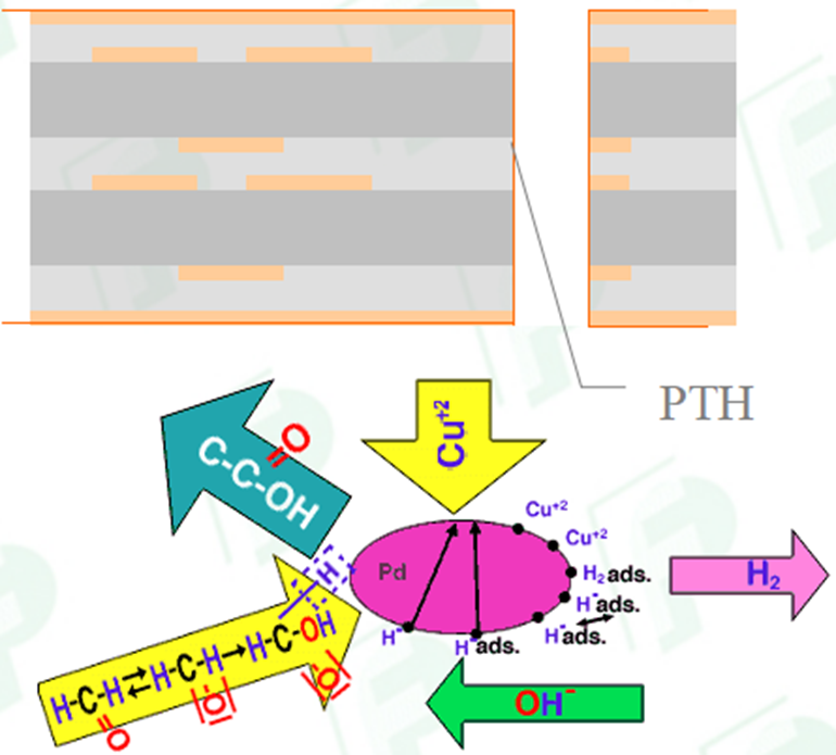
Chemical Copper (PTH):
Purpose of chemical copper: To deposit a thickness of 20-40 microinches of chemical copper through chemical deposition.
Changes in hole walls: As shown in the figure below.
Principle of chemical copper: As shown in the figure below.
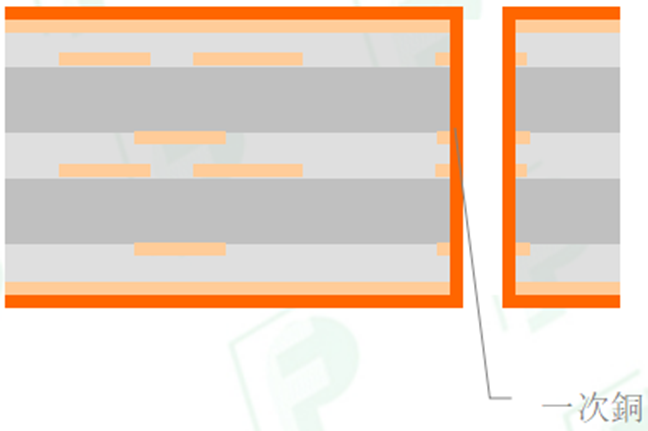
Electroplating Process – Copper Electroplating Introduction
First Copper:
Purpose of first copper: To plate a thickness of 200-500 microinches of copper to protect the only 20-40 microinch thick chemical copper from being damaged in subsequent processes.
Main production material: Copper balls.
D. Introduction to Outer Layer Dry Film Process
Process Introduction:

Purpose:
-
After drilling and through-hole electroplating, the inner and outer layers are connected; this process produces the outer layer dry film, providing graphics for the creation of outer layer circuits.
Outer Layer Dry Film – Pre-treatment Introduction
Pre-treatment:
Purpose: To remove contaminants from the copper surface and increase the roughness of the copper surface to facilitate the lamination process.
Main raw material: Scrubbers.
Lamination:
Purpose: To tightly adhere the dry film to the copper surface through heat pressing.
Main raw material: Dry film.
Outer Layer Dry Film – Exposure Introduction
Exposure (Exposure):
Purpose: To expose the required circuit on the dry film through graphic transfer technology.
Main raw material: Film.
Outer Layer Dry Film – Development Introduction
Development (DEVELOPING):
Purpose: To wash away the areas that have not undergone polymerization reaction with developing solution, while the photosensitive areas remain due to having undergone polymerization and act as etching or plating resist films.
Main production material: Weak alkali (K2CO3).
E. Introduction to Outer Layer Circuit Process
Process Introduction:

Purpose:
To plate copper to the thickness required by the customer.
To complete the circuit shape required by the customer.
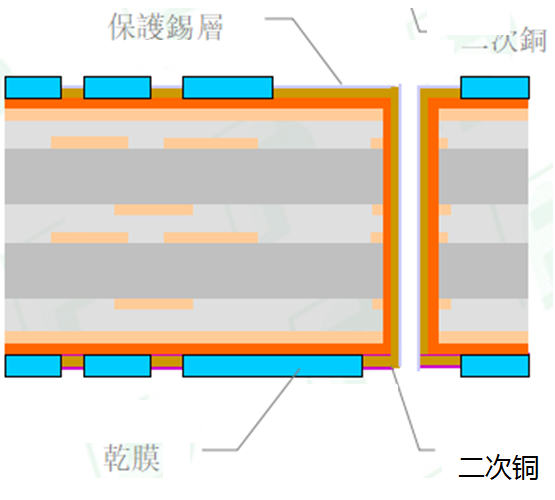
Outer Layer Circuit – Copper Electroplating Introduction
Second Copper:
Purpose: To increase the thickness of the exposed copper surface after development to meet the required copper thickness.
Main production material: Copper balls.
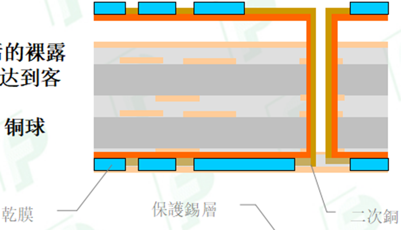
Tinning:
Purpose: To plate a layer of tin on the surface of the second copper as a protective agent during etching.
Main production material: Tin balls.
Outer Layer Circuit – Alkaline Etching Introduction
Stripping:
Purpose: To strip the dry film used for electroplating with chemicals.
Main production material: Stripping solution (NaOH).
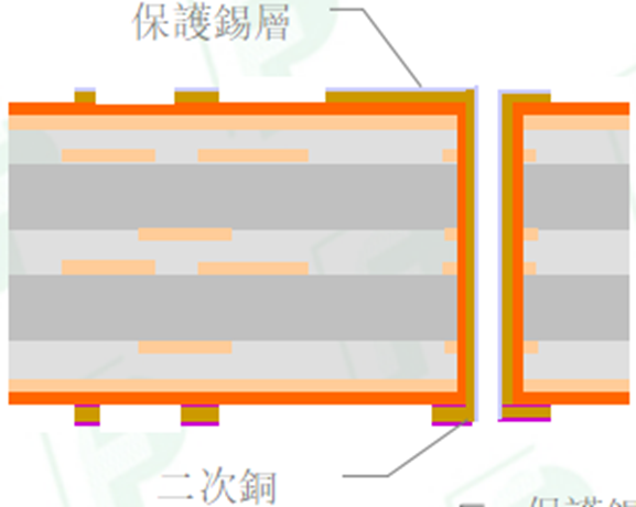
Circuit Etching:
Purpose: To etch away the copper from the non-conductive parts.
Main production materials: Etching solution, ammonia.
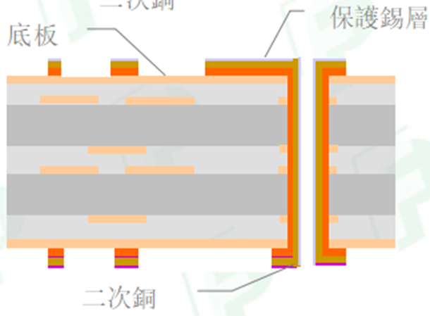
Outer Layer Circuit – Tin Stripping Introduction
Tin Stripping:
Purpose: To strip the tin that serves as a protective agent from the conductive parts.
Main production material: HNO3 tin stripping solution.
F. Introduction to Screen Printing Process
Process Introduction:

Purpose:
To provide a protective layer for the outer layer circuits, ensuring insulation and protection from soldering.
To create character markings.
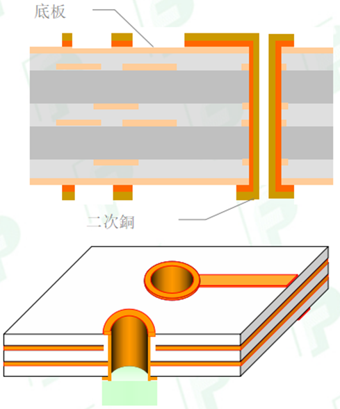
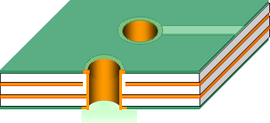
Screen Printing Process – Solder Mask Introduction
Solder Mask:
Solder mask, commonly known as “green oil,” is often mixed with green pigment in the main paint to facilitate visual inspection; other colors such as yellow, white, and black are also available.
Purpose:
A. Solder Mask: To leave through holes and pads on the board for soldering, covering all circuits and copper surfaces to prevent short circuits caused by wave soldering and to save solder usage.
B. Protection: To prevent moisture and various electrolytes from damaging the circuits and affecting electrical performance, and to prevent external mechanical damage to maintain good insulation of the board surface.
C. Insulation: As boards become thinner and line widths become finer, insulation issues between conductors become increasingly prominent, highlighting the importance of solder mask insulation performance.
Solder Mask Process Flow Chart
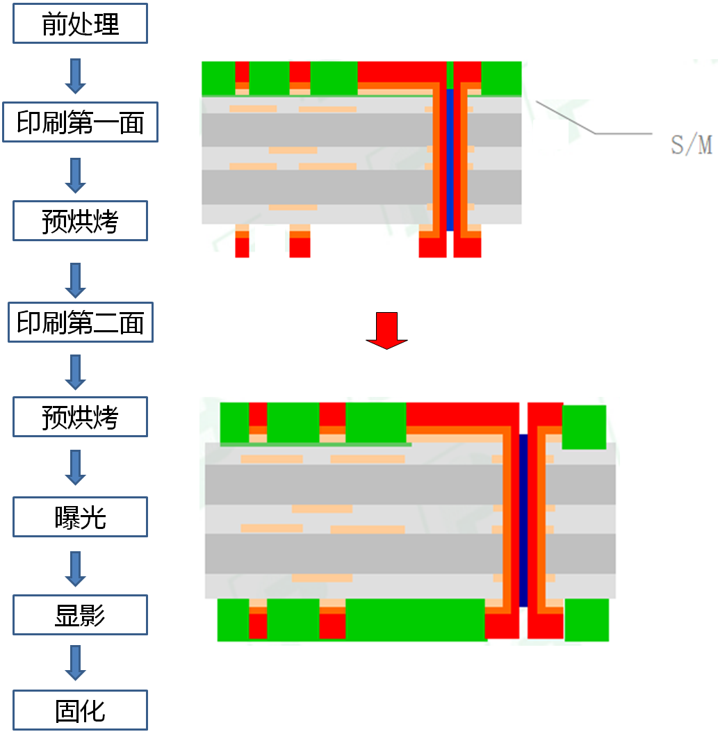
Solder Mask Process – Pre-treatment Introduction
Pre-treatment:
Purpose: To remove surface oxides, increase board surface roughness, and enhance ink adhesion to the board surface.
Main raw material: Volcanic ash.
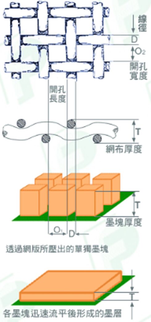
Printing:
Purpose: To print ink onto the board using a screen printing method, as shown on the right:
Main raw material: Ink.
Common printing methods:
A. Screen Printing
B. Curtain Coating
C. Spray Coating
D. Roller Coating
Solder Mask Process – Pre-baking Introduction
Pre-baking:
Purpose: To drive away solvents in the ink, allowing the ink to partially harden and preventing it from sticking to the film during exposure.
Key process points:
The temperature and time settings must refer to the conditions provided by the supplier; the pre-baking conditions for double-sided and single-sided printing are different.
The choice of oven must consider ventilation and filtering systems to prevent foreign matter from sticking.
The temperature and time settings must have alarms; once the time is up, they must be removed immediately; otherwise, over-curing may cause incomplete development.
Solder Mask Process – Exposure and Development Introduction
Exposure:
Purpose: To transfer the image.
Main equipment: Exposure machine.
Key process points:
A. Cleaning the exposure machine.
B. Selection of energy.
C. Control of vacuum.
Development:
Purpose: To remove the unpolymerized photosensitive ink using a 1% potassium carbonate solution.
Main production material: Potassium carbonate.
Character Process – Printing Introduction
Character Printing:
Purpose: To facilitate maintenance and identification.
Principle: Screen printing method.
Main production material: Character ink.

Character Process – Curing Introduction
Curing (Post-bake):
Purpose: To thoroughly cure the epoxy resin in the ink through high-temperature baking.
G. Introduction to Surface Process Selection
Conventional printed circuit boards (PCBs) have copper layers on the board, which, if unprotected, will oxidize and degrade, directly affecting subsequent soldering.
There are various protective layers available, the most common being: Hot Air Solder Leveling (HASL), Organic Solderability Preservative (OSP), Gold Plating, Electroless Nickel/Gold (ENIG), Gold Finger, Immersion Silver, and Immersion Tin.
(1) Hot Air Solder Leveling (HASL): The board is completely covered with solder, then excess solder on the surface and inside the holes is blown away with high-pressure hot air, leveling the solder attached to pads and hole walls; available in lead and lead-free options.
Advantages: Low cost, maintains solderability throughout the manufacturing process.
(2) Organic Solderability Preservative (OSP): To form a thin, uniform protective layer on the copper surface of the PCB.
Advantages: Comparable cost to HASL, good coplanarity, lead-free process.
(3) Gold Plating: To electroplate nickel and a protective gold layer on the copper surface.
Advantages: Good solderability, flat surface, long shelf life, withstands multiple reflow soldering.
(4) Electroless Nickel/Gold (ENIG): To replace the copper surface with a nickel-phosphorus layer through a chemical reaction, followed by a layer of gold on top.
Advantages: Good solderability, flat surface, long shelf life, withstands multiple reflow soldering.
(5) Gold Finger: To electroplate nickel and gold on the same surface, as the gold plating contains other metals.
(6) Immersion Silver (IS): To deposit a silver layer of 0.1 to 0.6 microns on the copper layer to protect the copper surface.
Advantages: Good solderability, flat surface, natural replacement for HASL immersion.
(7) Immersion Tin (IT): To deposit a tin layer of 0.8 to 1.2 microns on the copper layer to protect the copper surface.
Advantages: Good solderability, flat surface, relatively low cost.
H. Introduction to Post-Process Workflows
Process Introduction:

Purpose:
-
To complete processing according to customer specifications.
-
To perform bare board testing as per electrical performance requirements.
-
To conduct final quality audits before shipment.
Post-process Shaping Workflow Introduction
Shaping
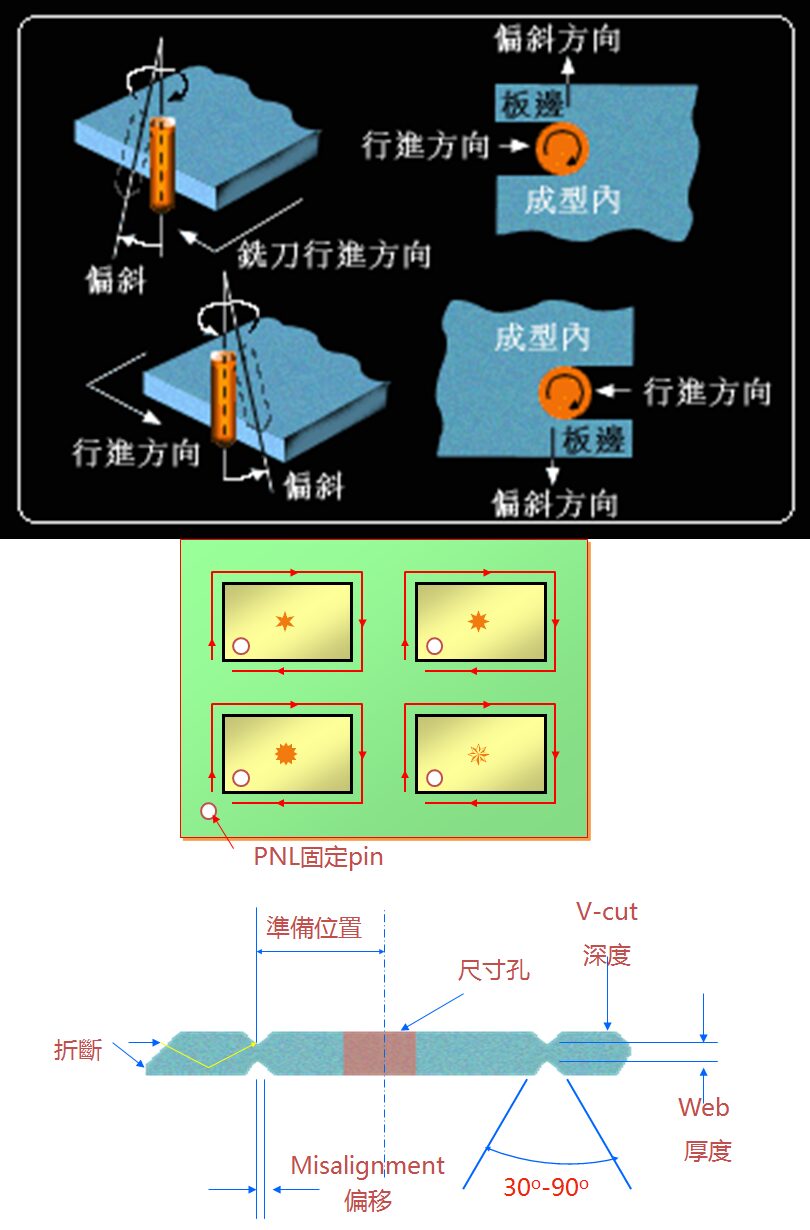
Purpose: To cut the board into the specifications required by the customer.
Principle: Digital machine tool mechanical cutting.
-
– Main production material: Milling cutter.
Post-process Electrical Testing Workflow Introduction
Electrical Testing
Purpose: To perform bare board testing for electrical performance, including open and short circuits, to meet customer requirements.
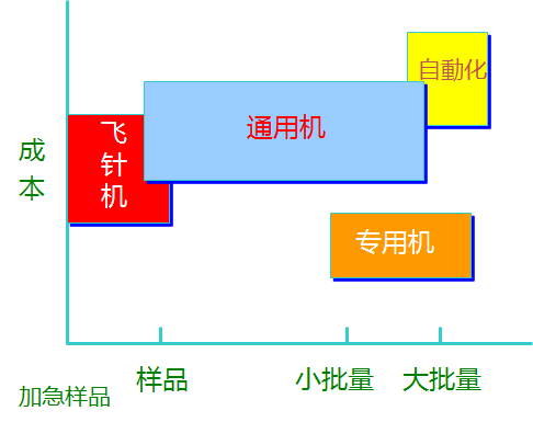
Types of electrical testing:
A. Dedicated machine testing
Advantages: Fast production speed.
Disadvantages: Test probes cannot be reused, and fixture costs are high.
B. Universal grid testing
Advantages: Lower fixture costs.
Disadvantages: High equipment costs.
C. Flying probe testing
Does not require expensive fixtures, using two probes to move in x, y, and z directions to test the endpoints of each circuit one by one.
Advantages: No fixture costs, low cost.
Disadvantages: Low efficiency.
Final Inspection/Laboratory Introduction
Final Inspection/Laboratory
Purpose: The final inspection/laboratory is the last quality check during the process.
(1) Main inspection items:
1. Outline Dimension
2. Hole to Edge
3. Board Thickness
4. Holes Diameter
5. Line width/space
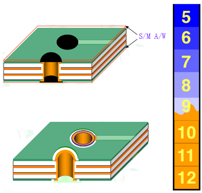
6. Annular Ring
And other appearance and length-related items!
(2) Main laboratory items:
1. Solderability
2. Peel strength
3. Micro Section
4. Thermal Shock
5. Ionic Contamination
6. Moisture and Insulation Resistance
7. Impedance
And other reliability-related items.
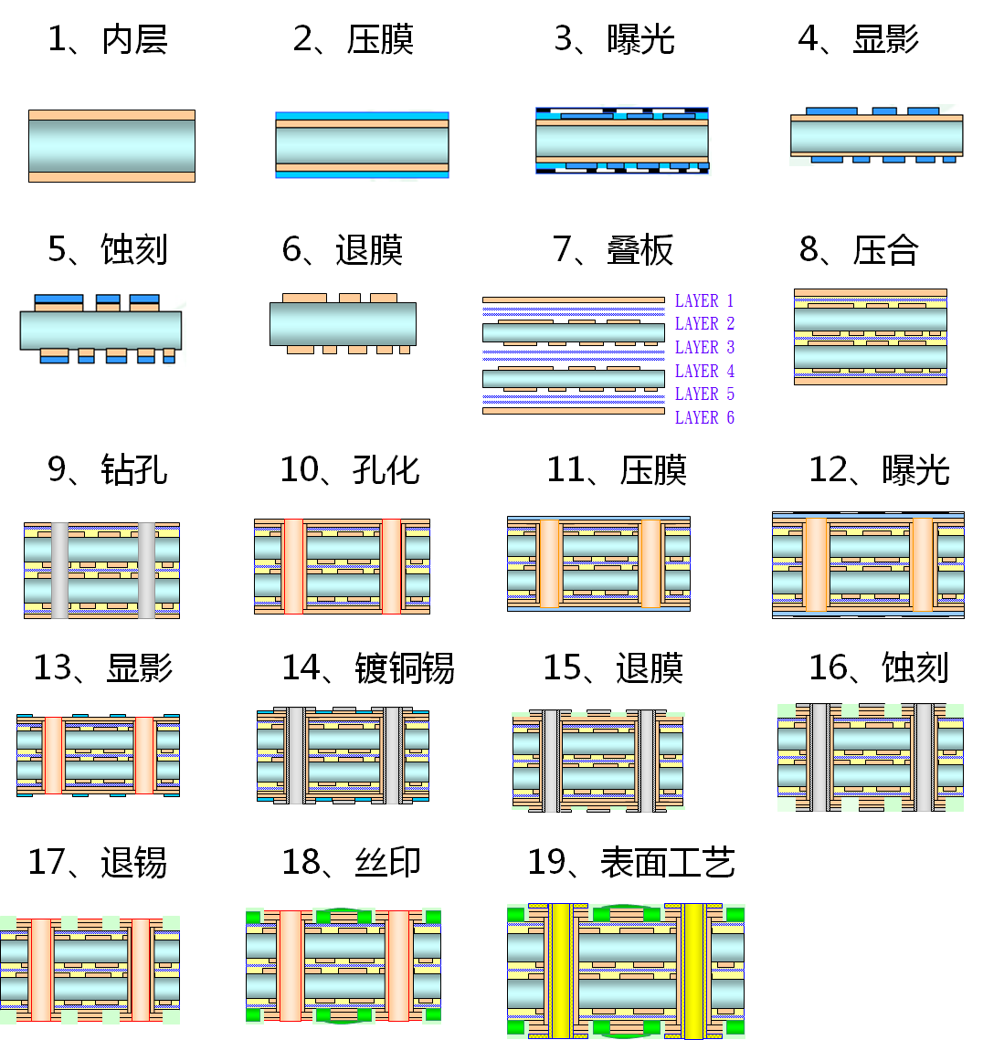
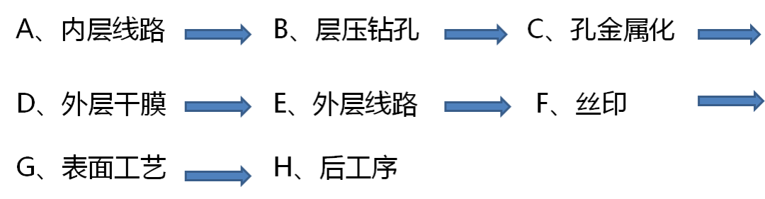
PCB Process Flow Diagram