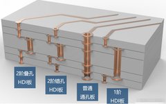
Understanding Multi-layer PCBs: A Comprehensive Guide

Understanding Multi-layer PCBs: A Comprehensive Guide

When hardware engineers first encounter multi-layer PCBs, it can be quite overwhelming. With sometimes ten or more layers, the layout resembles a spider web. Are you still struggling? Today, I’ve created several internal structure diagrams of multi-layer PCBs, using 3D graphics to display various stacking structures of PCB internal architecture, helping you to see clearly. … Read more

Essential Multi-layer PCB Design Techniques

Essential Multi-layer PCB Design Techniques

Remember when I first did PCB Layout, multi-layer board prototyping costs were very high, and the delivery time was about seven or eight days. Due to cost and time considerations, I often only considered using double-sided boards for routing. Then, holding many design rules that would often “conflict” with each other or experience-based rules circulating … Read more