Source: Old Thousand and His Friends
Original Author: Sun Qian
The printed circuit board (PCB) refers to a printed board that forms point-to-point connections and printed components on a common substrate according to a predetermined design. Its main functions are: 1) to provide mechanical support for various components in the circuit; 2) to create electrical connections between various electronic components, serving as a relay; 3) to mark the installed components with symbols for easy installation, inspection, and debugging.
PCBs enable the interconnection of electronic components, acting as a relay, and are the support structure for electronic components, hence they are referred to as the “mother of electronic products.” The manufacturing quality of PCBs not only directly affects the reliability of electronic products but also impacts the integrity of signal transmission between various chips. Therefore, the development level of the PCB industry reflects, to some extent, the technological level of the IT industry in a country or region.
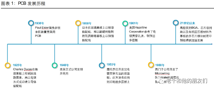
The technology of PCBs is closely related to the development of integrated circuit technology. With the rapid advancement of semiconductor technology, the PCB industry’s technology continues to improve and mature. Since the first use of PCBs in radios in 1936, PCB technology has undergone tremendous changes over nearly a century, evolving from single-sided boards to double-sided boards, and then to multi-layer boards; from through-hole technology to surface mount technology (SMT), and then to ball grid array packaging (BGA).
In terms of PCB processing technology, new process flows have been developed in areas such as pattern manufacturing, laser drilling, surface coating, and inspection. The application of blind holes, buried holes, and lamination methods has also become common, with high density and high performance becoming the direction of PCB technology development.
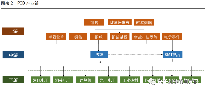
The upstream of the PCB industry chain consists of related raw materials, including copper-clad laminate (CCL), prepreg, copper foil, copper balls, gold salts, dry film, and ink. The midstream is PCB manufacturing, while the downstream mainly includes fields such as communication, consumer electronics, automotive electronics, industrial control, medical, aerospace, national defense, and semiconductor packaging.
In PCB operating costs, raw material costs are relatively high, often accounting for about 60%. Among these, CCL has the largest cost share, accounting for 30%, its importance is self-evident, followed by copper foil at 9%, copper balls at 6%, and ink at 3%. As the core substrate for PCB manufacturing, the three main raw materials for producing CCL include copper foil, resin, and fiberglass cloth. The conductivity, insulation, and support of PCBs mainly rely on these three raw materials, among which copper foil accounts for 42%, resin 26%, and fiberglass cloth 19%.
2 Who Invented PCB First?
Many people believe that Eisler invented the printed circuit board (PCB) in the mid-1930s, but in fact, its origins are almost 50 years earlier. If this is true, then who invented the printed circuit board? This article presents another perspective on the history of PCBs, including early developments and contributions from the fields of art and printing, innovations in science and engineering, and key developments in modern electronics.
Any study of the origins of printed circuit boards (PCBs) will typically find one name: Eisler. Paul Eisler’s first patent for PCBs was published in 1936 (Eisler and Williams, 1989), but according to patent searches conducted by Ken Gilleo (1992, 2003) and others, the origin of PCBs predates Eisler by nearly 50 years.
3 The Origin of PCBs
Baynes (1888) published a patent that was specifically designed for the art world at that time. This patent describes a method of etching patterns onto panels or other objects using an acid bath. Each panel has a pattern, similar to the principles of photography. During the etching process, Baynes found that the patterns had noticeable depressions. His solution was to first etch the outline, then coat the outline with wax or other etching resist. Then, the complete pattern would be etched, and finally, the protective layer would be removed.
12 years later, King (1900) proposed an improved version of the above method. To achieve this, a thin layer of silver needed to be deposited over the entire surface of the object. The desired pattern to be replicated as a metal film was first painted with watercolor, and then a resist such as asphalt was applied to the reverse image. After washing away the watercolor, the surface was prepared for the electrodeposition of the desired metal. Subsequently, the resist was removed, revealing the remaining silver.
Many later inventions seem to have been inspired by these two inventors, as their patents appeared in the citation lists of later numerous patents (Eisler, 1948; Nieter, 1955a, b; Rubin, 1948). Therefore, it can be said that the modern printed circuit board originated in the art world rather than the technology world.
4 Upgrading PCB Technology: From Art to Printing to Circuits
Before 1913, these processes were used for the manufacture of electronic circuits. Berry (1913) applied subtractive processes to produce electric heaters and described the “heating” bands. This can be interpreted as the first flexible circuit board.
In fact, 9 years before Berry, Hanson (1903) began researching methods to compactly arrange a large number of conductors to alleviate wiring congestion in telephone distribution boards. All designs used electrical wires and various insulating materials such as paper, gutta-percha, and cellulose. However, Hanson noted in his patent that he managed to “draw metal powder lines directly on the insulating material layer through electrodeposition or mechanical deposition in a suitable medium” to manufacture conductors. In hindsight, many so-called modern circuit concepts can be found in this patent. These concepts include double-sided through-hole circuits, multilayer circuits, high-density circuits, and another additive method different from the one described by King for producing circuit boards.
Chisholm (1915) focused on improving the manufacturing of lithographic plates. To achieve a more uniform, elastic, and tough surface, he used a method of electrodepositing copper followed by nickel deposition. To provide sufficient surface for the metal deposit, volatile solvents, fine metal powders, and porous substrates were used. The precursors of conductive pastes and inks?
The next important inventor was Charles Ducas. His patent (Ducas, 1925) was cited by at least five other patents (Eisler, 1948; McLarn, 1947; Nieter, 1955a, b; Rubin, 1948), which contain many transformations based on one method. This method sought alternative ways to produce conductors to avoid winding single-strand wires. Various methods were used to create metallized designs on insulating materials. Then, panels containing metallized circuits were electroplated to deposit the required amount of metal. The methods for making panels varied, including the following:
Ø Exposing the desired design’s metal on the substrate using a lathe. The substrate is made of conductive material coated with a non-conductive layer.
Ø Transferring the image to a blank panel using conductive paste.
Ø Printing the image in wax or other low-melting materials, and then coating with conductive material.
Ø Using conductive paste and any printing method to create the desired image.
Charles Ducas also mentioned that conductors could be made on both sides of the insulating substrate and introduced a method of connecting layers together using conductors extending through holes to the other side. This implied multilayer circuits, but the inventor did not elaborate further.
5 Commercialization of PCBs and Modern Processes
In 1926, César Parolini from France made the first attempt to produce complete circuits using the additive method based on the concepts proposed by earlier inventors. Figure 1 shows printed circuits using U-shaped metal pieces, which act as bridges at track intersections. The use of bridges makes the design more compact. Ink dipped in metal powder was used to create the tracks. After bridging, the panel was electroplated until the desired metal thickness was reached.
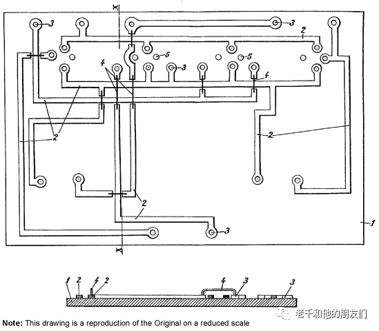
Circuit layout: Design from César Parolini
In 1927, Frederick Seymour published a general patent specifically concerning the manufacture of flexible circuits, and he also proposed the concept of three-dimensional circuits (Seymour, 1927). This patent describes the process of producing inductors, which were reduced in size but not in function. This was achieved through “any well-known means”: using any conductive material to draw patterns on flexible boards.
Erwin Franz built upon the ideas of Parolini and Seymour and published this achievement in 1935. A bonding medium containing graphite or metallic pigments in ink was used to depict images on dielectric materials. The transfer method could be printing, molding, peeling, or using transfer rollers. The panel was then electroplated to achieve the desired thickness of metal. The patent noted that different track widths would lead to corresponding changes in electroplating thickness, but no remedies were proposed.
The Saint-Gobain company researched a completely different area between 1939 and 1942 (Loiseleur, 1942; Société Anonyme des Manufactures des Glaces et Produits Chimiques de Saint Gobain, 1939). The company was developing a method of metal deposition that did not require an external power source. This method was only applicable to metals such as copper and silver, as these metals have positive electrode potentials relative to hydrogen. To obtain a metal film, it was necessary to use “a solution containing metal salts to be deposited” and “an alkaline solution of this salt, which also contains ferrous salts and hydroxy acids.” This description covers the basic chemicals listed in the examples and can be considered the first description of what is now referred to as electroless solutions.
At this time, circuit board manufacturers were trying to leverage the development of new, inexpensive substrate materials known as “plastics.” If existing methods were used, the circuits produced would have poor adhesion between the metal and the substrate. Walker (1940) referred to the adhesion problem as “depolymerization” and set out to solve it. He believed that to achieve good adhesion, physical and chemical changes must occur on the surface. He used a solution containing stannous chloride (later known as a sensitizer) to make the substrate more susceptible to the chemicals used later, thereby improving the bonding strength between the substrate and the metal. This seems to be the earliest mention of using a sensitizer to improve adhesion. It paved the way for further developments in the pretreatment of substrates for chemical plating and/or electroplating, as seen in the studies by McLarn (1947) and Narcus (1948).
McLarn’s patent (1947) describes a process still in use today: transferring the circuit image onto the substrate using electronically conductive ink through rubber stamps or printing plates. The actual ink formulation is not provided. In addition to the circuit design, connecting lines need to be added to connect all tracks together, as well as adding tracks as contact points for electroplating. The panel is then electroplated to the desired thickness. During disassembly, the panel is cleaned, and unnecessary lines and connections are cut and removed if necessary.
Just like the new design process described by McLarn, Narcus (1948) also began to offer an alternative method of using silver as a coating before electroplating. Using silver posed many problems, including high cost, low adhesion, and the formation of silver oxide leading to uneven electroplating. To address this issue, Narcus developed an improved activator and chemical plating solution.
The pretreatment before chemical plating includes two solutions: one is an activation solution, and the other is a seeding solution. The chemicals required for the activation solution used in the example include titanium oxide, sulfuric acid, sodium dodecyl sulfate, and water. The panel is then rinsed and immersed in a seed solution made of palladium chloride, hydrochloric acid, and water. No further rinsing is needed, and the panel is placed into the electroless solution. This solution is made by mixing the two solutions.
The chemicals listed in the example are as follows, with alternatives in parentheses.
Solution A
Ø Copper fluoroborate (any copper salt);
Ø Nickel fluoroborate (similar salts of metals that are positioned higher than hydrogen in the electrochemical series);
Ø α-trimethylol (formaldehyde);
Ø Water.
Solution B (carrying solution, with various forms)
Ø Sodium hydroxide;
Ø Rochelle salt;
Ø Sodium carbonate.
After mixing, the panel is immersed in water for 30-40 minutes, with the first copper deposition appearing after 5 minutes. The panel is then thoroughly rinsed before electroplating. Here, Walker (1940) and Saint-Gobain’s patents are referenced, but significant modifications have been made to the original ideas and formulations. This is to be expected, as about 10 years have passed since the initial patent application.
6 Mass Production of PCBs
It was during this period that Paul Eisler first appeared in the PCB field, with his main contribution being the successful transition from laboratory scale to full-scale production. This began in 1941 when a company named Technograph Printed Circuits Limited was established in London, of which Eisler was one of the directors. After achieving success in the UK, attention shifted to the USA, and a sister company was established in 1949. A few years later, the situation worsened, and Eisler became increasingly disappointed with the development direction of the UK company. However, it was this sister company that was destined to spiral Eisler’s personal dreams and ambitions for “his” printed circuit board invention downward.
Among Eisler’s various patents, the US patent (Eisler, 1948) is particularly noteworthy due to its citation list. This US patent contains most of the details regarding PCBs found in Eisler’s earlier UK patents. The citation list includes the patents of Baynes, Ducas, and Seymour, which were used as evidence in a lengthy trial that concluded in 1963. In this trial, the US Technographic Printed Circuits Inc. sued Bendix for patent infringement. Bendix had more resources and attempted to invalidate the printed circuit concept proposed by Eisler using the patents of the aforementioned inventors.
The judge ruled in favor of Bendix, declaring several of Eisler’s patents invalid (Eisler and Williams, 1989). The US Patent Office took 4 years to initially approve Eisler’s application, citing multiple mentions of “well-known printing techniques” or similar phrases. Ironically, Seymour also used similar phrases, but these phrases were used as evidence against Eisler.
Eisler felt he was subjected to institutional injustice. He believed his patents were sufficient to defend in court. He and his patent attorney “almost knew all the citations of existing technologies and were very careful to perfect the patent documents” (Eisler and Williams, 1989). However, the outcome of this court case seemed to indicate otherwise.
During the same period, Ott (1950) described enamels that appeared in multiple colors, which were specifically used in the art world as decorative etching resists and remained on the final product. The glazes used were mainly based on alkyd resin and organic pigments. Organic pigments seemed to be the source of color. The components that made up the enamel are similar to some of the components currently used to produce conductive films, which are used in the additive production of PCBs. In addition, Ott’s preferred application method was ordinary printing or screening methods, which aligns with modern preferences.
7 Motorola
In 1953, Motorola developed a pioneer of the modern semi-additive process (Coombs, 1996), known as the placir (PLAted CIRcuitry) method. This process was one of the earliest through-hole plating (PTH) technologies. It was developed by Motorola with the aim of reducing the costs of radios.
The patent obtained by Motorola (Nieter, 1955) is identical in process, differing only in that the latter patent applies to the plating of holes, namely PTH. These patents aimed to address the issues of insufficient shielding materials and the defects caused by chemicals used to remove silver on the tracks. At that time, the use of photosensitive materials to transfer resists did not fully protect the surface effectively.
The proposed solution was to drill holes in the panel, sensitizing it with stannous chloride, and then spraying a dual solution of silver salts and reducing solutions to produce metallic silver. The surface was then printed with the negative image of the film using screen printing technology, as screen printing allows for a thicker resist layer to be printed at once compared to other printing methods. After completion, the panel was electroplated to achieve the desired thickness of copper. After rinsing, the resist layer was removed, and then silver was plated.
It may be easy to see the similarities between this patent and earlier patents. In fact, among the citation lists of these two patents, nine were previously described patents. However, this indicates that although recent improvements in electroless solutions have been made, they were still not sufficient for use in mainstream production, and the use of silver and etching remained the mainstream process at that time.
8 The Focus Shifts: Copper Replaces Silver?
As silver became increasingly expensive, the demand for better adhesion grew, and research began to focus more on improving electroless solutions and the pretreatment stage, often replacing silver with copper. The Shipley family established a company in Newton, Massachusetts, which was destined to have a significant impact on the manufacture of printed circuit boards.
The company’s initial business focus was on designing and manufacturing equipment for the industry. After a while, they realized that there was a greater market demand for specialty chemicals, especially for chemicals used in the PTH process. It was well known that the sensitizing baths used at that time were essentially unstable and unpredictable (Shipley, 1961). After extensive research, Shipley Company discovered a single-step catalyst in 1958, which could produce good through-hole plating on a new type of substrate known as copper-clad laminate. Before this invention, attempts were made to use old catalyst steps on the new series of substrates, leading to poor adhesion between copper foil and electroless copper (Coombs, 1996).
In the relevant patent (Shipley, 1961), the catalysts used for illustration included palladium chloride, water, concentrated hydrochloric acid, and stannous chloride. This combination of chemicals is still in use today. This new catalyst was still not enough to convince manufacturers to use electroless copper instead of silver. While the stability and effectiveness of the catalyst may have improved, the stability of the chemical solution itself remained an issue.
9 Refining the Chemical Plating Process
In the late 1950s, many were working to develop an electroless solution to be used in conjunction with improved catalysts. Atkinson was reported to be the winner of this race (Coombs, 1996). The gap of 8 years between the application date and publication date seems to prove this, as it took so long to organize all the different applications to find the true viable invention (Atkinson, 1964).
The use of chelating agents, changes in the pH of the plating solution, and the addition of wetting agents allowed the plating solution to remain stable for about 8 hours. Chelating agents keep copper in solution by wrapping metal ions, but under appropriate conditions, chelating agents release copper to allow deposition to occur. Two chelating agents are mentioned here, but the main one currently used is ethylenediaminetetraacetic acid (EDTA).
Sodium hydroxide provides the required pH, while trisodium phosphate acts as a buffer. Formaldehyde remains the reducing agent in previous formulations. The wetting agent is not easily identified, but it allows copper to deposit uniformly on the panel surface. The pretreatment stage used in this patent has been replaced by Shipley’s one-step catalyst, which was developed during the waiting period for this patent’s approval.
After 8 years of refining the electroless solution, Zeblisky (1972) improved the Shipley catalyst. When using the Shipley catalyst in industry, it was found that the immersion time needed to be longer than previously anticipated for good copper coverage. Additionally, there were issues with reaction activity declining over shorter periods.
These improvements also involved using a combination of two metals and an anion within a specific ratio range. The preferred metals are palladium and tin, with chloride ions as the anionic component. These components are dissolved in an acidic solution. It is best to select an acid that matches the anion of the metal salt used.
The original process had good adhesion in the holes, but poor adhesion elsewhere. Before this invention, using “glass paper tape” would cause the plated copper to separate from the metal foil unless the electroless copper was removed beforehand. Different degrees of adhesion were caused by the substrate materials. The substrate for the holes was laminate, while the rest of the circuit board was copper foil. Improvements in the catalyst/sensitizer have increased the adhesion between copper foil and chemical copper, eliminating the need to remove chemical copper.
With this development in 1972, the catalyst, electroless copper, and electroplated copper bore more resemblance to the solutions used today. In recent years, the focus has been on modifying these basic formulations to meet the specifications of the final products.
10 The Modern History of PCBs
Utilizing this chemical composition, David Harrison, Blue Ramsey, and Peter Evans from Brunel University’s Department of Design and Systems Engineering began exploring the possibility of using additive methods and lithography to manufacture printed circuit boards (Harrison et al., 1997). Since then, three generations of lithographic inks have been invented. The first generation is conductive ink, the second generation is “seeding” ink, and the third generation ink is a cost-effective alternative to the second generation “seeding” ink. The active materials in the first two inks are silver, while the third is copper oxide.
Conductive ink can be used immediately after lithographic printing. It has been shown to be suitable for low-end products such as RFID devices, reflecting a shift in the factors influencing process selection from quality, durability, and reliability to cost, flexibility, and efficiency (Allardyce, 1996).
The next two generations of products need to be processed with chemicals similar to those used in traditional PCB manufacturing to achieve the desired copper deposition. The invention of these two inks is based on the combination of the ink with subsequent pretreatment stages. This method shortens the pretreatment time. The transition from the photoresist stage to the lithographic printing stage significantly reduces this time, allowing additive methods to have a wider application than before.
The development of additive methods for printed circuit boards has so far made slow progress in commercial-scale applications.
Until recently, market conditions were still unfavorable for the PCB industry to adopt any new, potentially disruptive technologies, thus hindering the adoption of additive processes. Due to economic recession, significant production capacity in the US and Europe has been eliminated or transferred to China, and the PCB industry is just beginning to slowly recover. Coupled with increasing regulations and legislation regarding health, safety, and the environment, it can be seen that the conditions for adopting additive processing methods are beginning to become favorable. Direct metalization has appeared at different times in the modern history of printed circuit boards.
In the 1990s, there was a strong interest in the so-called direct metalization process, which was seen as an alternative process to electroless copper. These processes are often praised as “new electroless” processes, and industry insiders are scrambling to switch to these processes. However, it can also be said that interest in these processes has waned, and the use of advanced electroless copper processes is continually being updated.
Before the electroless solutions stop developing to address emerging problems/concerns, direct metalization processes may remain in a secondary position. Perhaps the ongoing concern over health risks associated with formaldehyde, as well as the difficulty in finding suitable alternative reducing agents, may again pave the way for direct metalization. Only time will tell if electroless methods can again “surprise” and secure their future.
11 Conclusion
Now, the process of development and evolution of PCBs is basically clear, and future development directions can be speculated. It has been proven that PCBs were not invented by one person but were jointly accomplished by a group of people, some of whose ideas were ahead of their time. For example, McLarn described a process that is very similar to Brunel’s new process steps, Hanson proposed ideas for producing double-sided through-holes, multilayer, and high-density circuits, and Seymour’s three-dimensional circuits. Although it has been proven that Eisler did not invent the printed circuit board as he believed, we cannot overlook his contributions. He successfully achieved the difficult transition from small-scale production to large-scale production, bringing printed circuit boards to the attention of the world. Without Eisler, the achievements of countless inventors before him would never have been recognized.
Ultimately, the success of PCBs, and even their continued success, is due to the contributions of different individuals from various fields. Coupled with favorable market conditions for adopting new technologies, perhaps it is time for a significant transformation in the manufacturing methods of printed circuit boards.
END
The reproduced content only represents the author’s views
It does not represent the position of the Institute of Semiconductors, Chinese Academy of Sciences
Editor: Schrödinger’s Cat
Editor-in-Charge: Jiang Yu
Submission Email: [email protected]
1. The Institute of Semiconductors has made progress in the research of bionic covering neuron models and learning methods
2. The Institute of Semiconductors has made significant progress in inverted structure perovskite solar cells
3. A Ten Thousand Word Review of the Semiconductor Development History of New China – “With great effort for decades, the light boat has passed through thousands of mountains”
4. What exactly is the 7nm chip?
5. Silicon-based integrated optical quantum chip technology
6. How abnormal is the quantum anomalous Hall effect? It may lead to the next information technology revolution!