Welcome FPGA engineers to join the official WeChat technical group
ClickBlue TextFollow us at FPGA Home – the largest and best FPGA community for pure engineers in China
1.Software and Hardware Platforms
Software Platform:
1. Operating System: Windows-8.1
2. Development Suite: ISE14.7
3. Simulation Tool: ModelSim-10.4-SE
Hardware Platform:
1. FPGA Model: XC6SLX45-2CSG324
2. USB to UART Chip: Silicon Labs CP2102GM
2.Principle Introduction
The serial port is short for serial interface, also known as serial communication interface or COM interface. Serial communication refers to a communication mode that transmits data one bit at a time over a single signal line using a serial communication protocol. Serial ports are classified according to electrical standards and protocols, including RS-232, RS-422, RS485, etc. Among them, the most commonly used is the RS-232 interface.
The RS-232 interface has the following three characteristics:
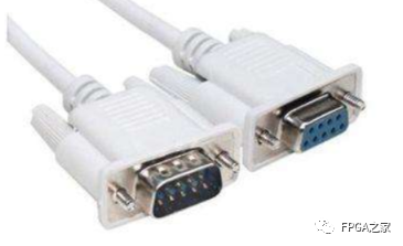
1. It uses a 9-pin connector “DB-9” (earlier computers used a 25-pin connector “DB-25”)
2. It allows full-duplex communication (i.e., data can be sent and received simultaneously via the serial port)
3. The maximum communication rate is about 10KBytes/s
The physical diagram of the DB-9 interface is shown below (this interface can be seen at the back of early computer hosts, and now USB to serial cables are generally used for serial communication):
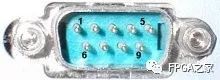
Although the DB-9 connector has a total of 9 wires, only 3 wires are needed to implement serial communication, which are:
1. pin-2: RXD (receive data), receives serial data
2. pin-3: TXD (transmit data), sends serial data
3. pin-5: GND (ground), ground wire
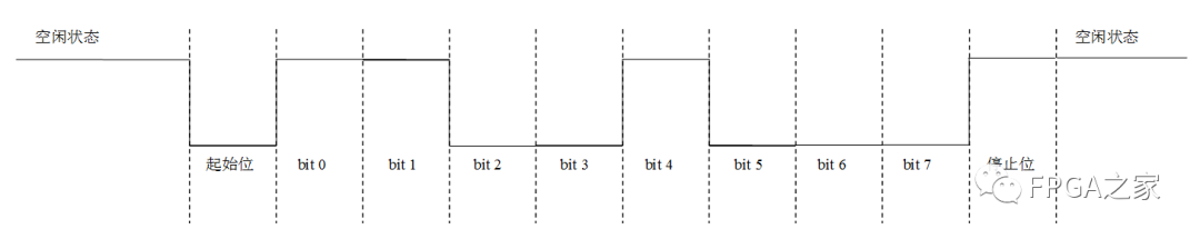
In serial communication, data is transmitted on a single line with a width of 1 bit, and one byte of data is divided into 8 transmissions, sent in order from the least significant bit to the most significant bit. This process is called the “serialized” process of data. Since serial communication is an asynchronous communication protocol, there is no clock signal transmitted with the data. When idle (no data transmission), the serial transmission line is at a high level of 1, so before the sender transmits a byte of data, it first sends a low level of 0. After the receiver receives this low level of 0, it knows that data is coming and prepares to start receiving data, thus achieving a communication. The timing of serial communication is shown in the figure below:
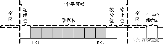
The specifications for serial communication are as follows:
1. In the idle state (no data transmission), the serial transmission line is at a high level of 1
2. The sender sends a low level of 0 to indicate the start of data transmission, this low level represents the start bit of transmission
3. The 8-bit data (1 Byte) is sent starting from the least significant bit, and the most significant bit is sent last
4. After the highest bit of the data is sent, the next bit is the parity bit, this bit can be omitted, and when the parity bit is not sent, the receiver also does not receive the parity bit
5. The last bit is the stop bit, indicated by a high level of 1
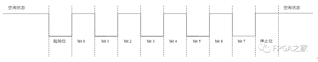
Below is an example of sending the byte 0x55 to illustrate the entire sending process:
First, convert 0x55 to binary: 01010101. Clearly, the least significant bit bit 0 is 1, the next least significant bit bit 1 is 0, …, the most significant bit bit 7 is 0, since the serial port sends a byte starting from the least significant bit, the sending order of each bit of 0x55 is 1-0-1-0-1-0-1-0, the waveform is shown in the figure below
Next, here is a waveform, based on the above rules it can also be easily determined that this is the waveform of sending the byte 0x13
The next question is: what is the speed of serial transmission?
In fact, the speed of serial transmission is specified by the baud rate. The baud rate indicates the number of bits sent per second, measured in bps (bits-per-seconds). For example, 1000 bauds means 1000 bits are sent in one second, or each bit lasts for 1ms. The baud rate for serial transmission has a set of standard specifications and is not just any number. Common baud rate standards include:
1. 1200 bps
2. 9600 bps (commonly used)
3. 38400 bps
4. 115200 bps (commonly used and usually the fastest baud rate we can use)
When the baud rate is 115200 bps, the duration of each bit is (1/115200)=8.7us, so sending 8 bits (1 Byte) takes 8*8.7us=69us. Not considering the parity bit, sending one byte also requires sending an additional 1 start bit and 1 stop bit, so the actual minimum time required to send 1 byte is 10*8.7us=87us, which means that in 1s (1000000us) about (1000000/87) = 11494 bytes can be sent, so at a baud rate of 115200bps, the serial transmission rate is about 11.5KB/s. However, some computers’ serial ports may sometimes require a longer stop bit, such as 1.5 or 2 stop bits, in which case the time taken to send a byte will be longer than when there is only one stop bit, resulting in a transmission rate lower than 10.5KB/s.
After summarizing the above series of points, we can conclude that serial communication between the FPGA and PC mainly includes three modules: the baud rate generation module, the transmission module, and the reception module.
3.Target Functions
1. Write the Verilog code for the transmission module and continuously send data from 0x00 to 0xff to the PC, where the PC receives and displays it in hexadecimal using a serial debugging assistant
2. Based on the first function, write the Verilog code for the reception module. After the reception module receives the data sent by the transmission module in the first function, it drives the four LED lights on the board using the lower four bits of the received parallel data
3. Write a top-level module that instantiates both the transmission module and the reception module, then sends data from the PC’s serial debugging assistant to the FPGA. After the FPGA receives the data, it returns the received data to the serial debugging assistant for display
4.Design Ideas andVerilogCode Writing
4.1、Design and Implementation of Baud Rate Clock for Transmission Module
This section illustrates the design method of the baud rate module using a baud rate of 115200bps as an example; other baud rates can be inferred similarly. Since the clock on my development board is 50MHz, the period T=20ns, and the baud rate is 115200bps, the duration of 1 bit is 8.7us, so the number of cycles occupied by each bit N=(8.7us / 20ns) = 434. Therefore, we can define a counter that resets when it counts from 0 to 433, and when the count value is 1 (this count value should ideally be less than half of 433, the reason for this is analyzed in the last part of this blog), a high pulse is generated. The transmission module only needs to detect the arrival of this high pulse to send a bit, thus achieving a baud rate of 115200bps for serial data transmission.
The logic for generating the baud rate clock for the reception module is slightly different from that for the transmission module. The difference is that when the reception module detects the falling edge of I_rs232_rxd, it indicates that data is coming, and it is ready to receive data. Since the duration of one bit is 434 clock cycles, to ensure the accuracy of the reception module in receiving data, we need to receive the input data at the midpoint of 434/2=217 cycles, meaning the baud rate clock for the reception module should lag behind the baud rate clock for the transmission module by several cycles.
The block diagram of the baud rate generation module is shown in the figure below:
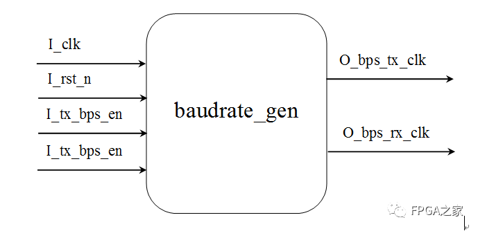
Where:
I_clk is the system clock;
I_rst_n is the system reset;
I_tx_bps_en is the transmission module baud rate enable signal. When I_tx_bps_en is 1, O_bps_tx_clk will output a clock signal;
I_rx_bps_en is the reception module baud rate enable signal. When I_rx_bps_en is 1, O_bps_rx_clk will output a clock signal.
The complete code for the baud rate module is as follows:

module baudrate_gen
(
    input   I_clk                  , // System 50MHz clock
    input   I_rst_n                , // System global reset
    input   I_bps_tx_clk_en        , // Serial port transmission module baud rate clock enable signal
    input   I_bps_rx_clk_en        , // Serial port reception module baud rate clock enable signal
    output  O_bps_tx_clk           , // Transmission module baud rate generation clock
    output  O_bps_rx_clk             // Reception module baud rate generation clock
);

parameter       C_BPS9600         = 5207         ,    // Baud rate 9600bps
                C_BPS19200        = 2603         ,    // Baud rate 19200bps
                C_BPS38400        = 1301         ,    // Baud rate 38400bps
                C_BPS57600        = 867          ,    // Baud rate 57600bps
                C_BPS115200       = 433          ;    // Baud rate 115200bps

parameter       C_BPS_SELECT      = C_BPS115200  ;    // Baud rate selection

reg [12:0]  R_bps_tx_cnt       ;
reg [12:0]  R_bps_rx_cnt       ;

///////////////////////////////////////////////////////////
// Function: Baud rate clock generation logic for serial port transmission module
///////////////////////////////////////////////////////////
always @(posedge I_clk or negedge I_rst_n)
begin
    if(!I_rst_n)
        R_bps_tx_cnt <= 13'd0 ;
    else if(I_bps_tx_clk_en == 1'b1)
        begin
            if(R_bps_tx_cnt == C_BPS_SELECT)
                R_bps_tx_cnt <= 13'd0 ;
            else
                R_bps_tx_cnt <= R_bps_tx_cnt + 1'b1 ;
        end
    else
        R_bps_tx_cnt <= 13'd0 ;
end

assign O_bps_tx_clk = (R_bps_tx_cnt == 13'd1) ? 1'b1 : 1'b0 ;

///////////////////////////////////////////////////////////
// Function: Baud rate clock generation logic for serial port reception module
///////////////////////////////////////////////////////////
always @(posedge I_clk or negedge I_rst_n)
begin
    if(!I_rst_n)
        R_bps_rx_cnt <= 13'd0 ;
    else if(I_bps_rx_clk_en == 1'b1)
        begin
            if(R_bps_rx_cnt == C_BPS_SELECT)
                R_bps_rx_cnt <= 13'd0 ;
            else
                R_bps_rx_cnt <= R_bps_rx_cnt + 1'b1 ;
        end
    else
        R_bps_rx_cnt <= 13'd0 ;
end

assign O_bps_rx_clk = (R_bps_rx_cnt == C_BPS_SELECT >> 1'b1) ? 1'b1 : 1'b0 ;

endmodule
The simulation of the baud rate module is as follows:
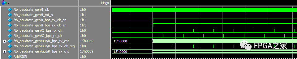
When the transmission baud rate clock enable signal is turned on, a transmission clock pulse is generated only after the count value reaches C_BPS_SELECT, while the reception baud rate clock generates a clock pulse after counting half of C_BPS_SELECT, which leads to O_bps_tx_clk lagging behind O_bps_rx_clk during the echo experiment. In the echo experiment, we directly connect the reception completion flag to the transmission start flag, so this may lead to the situation where the previous data has not been fully sent when the new data arrives. Through my testing, using the above baud rate logic generally works well if there is no echo experiment. However, in the case of the echo experiment, at higher baud rates like 115200bps and 57600bps, with smaller amounts of data, there are usually no errors, but with larger amounts of data, there is generally data loss. At lower baud rates like 9600bps and 2400bps, data is received frame by frame, for example, when sending the string abcdef, the received result is ace. I discovered this reason using ChipScope. Please pay attention to this issue in the future.
5.2、The state machines for sending and receiving data can be implemented using shifting methods
In fact, the state machines for sending 8-bit data and receiving 8-bit data can be implemented using shifting methods, which would make the code shorter and more refined. I will rewrite this when I have time.

Welcome engineers in FPGA and embedded systems to follow our public account

National Largest FPGA WeChat Technical Group
Welcome everyone to join the national FPGA WeChat technical group, which has tens of thousands of engineers, a group of engineers who love technology. FPGA engineers here help each other, share knowledge, and have a strong technical atmosphere!Hurry up and invite your friends to join!!

Press and hold to join the nationwide FPGA technical group
FPGA Home Components City
Advantageous components services, please scan the code to contact the group owner: Jin Juan Email: [email protected] Welcome to recommend to procurement
ACTEL, AD part of advantageous ordering (operating full series):
XILINX, ALTERA advantageous stock or ordering (operating full series):
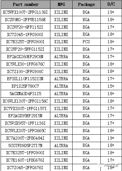
(The above devices are partial models, for more models please consult the group owner Jin Juan)
Service concept: FPGA Home Components City aims to facilitate engineers to quickly and conveniently purchase components. After several years of dedicated service, our customer service covers large listed companies, military research institutes, and small and medium enterprises across the country. Our biggest advantage is emphasizing service first, and ensuring fast delivery and favorable prices!
Directly operated brands: Xilinx ALTERA ADI TI NXP ST E2V, Micron and other hundreds of component brands, especially good at handling components under US embargo against China,Welcome engineer friends to recommend us to procurement or personally consult us!We will continue to provide the best service in the industry!

FPGA Technical Group Official Thanks to Brands: Xilinx, Intel (Altera), Microsemi (Actel), Lattice, Vantis, Quicklogic, Lucent, etc.