Step-by-Step Guide to Designing an FIR Digital Filter with FPGA
Requirements
Design a bandpass filter and verify its functionality.
1. Use MATLAB to Design Filter Coefficients
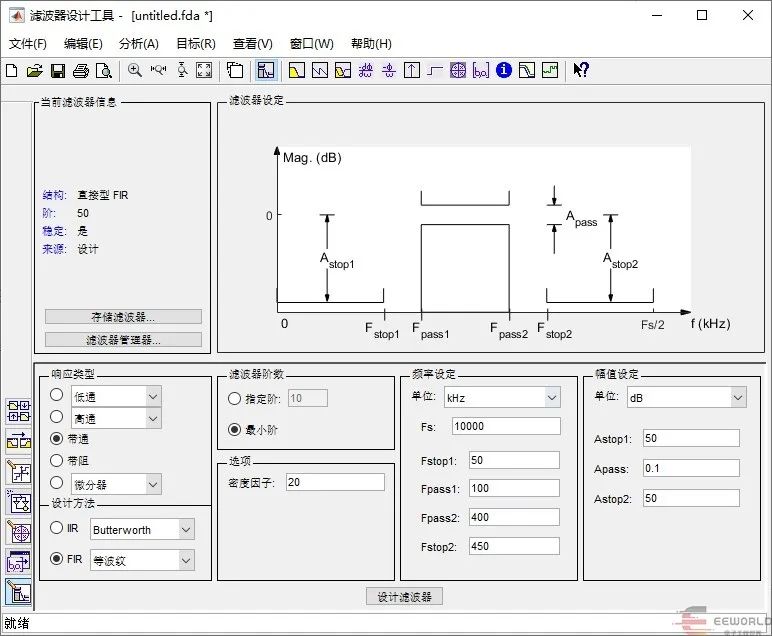
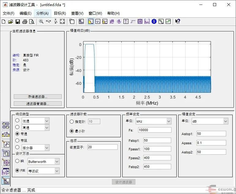
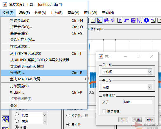
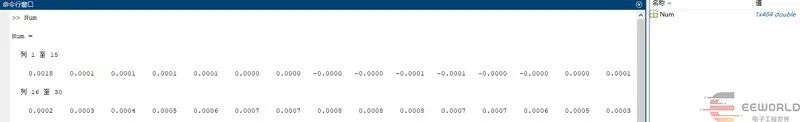
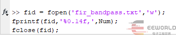
Find the Filter Design Tool on the MATLAB homepage after locating the APP, and use this tool to generate the coefficients for the digital filter, which will later be used to configure the FIR IP core on the FPGA.After opening the Filter Design Tool, you can input the relevant parameters and design the required filter. For this design, we are creating a bandpass filter, so select ‘Bandpass’ as the filter response type; choose ‘FIR’ (Finite Impulse Response) for the design method; for the filter order, select the minimum order, but you can specify a custom order if needed. A higher order results in better filtering but consumes more FPGA resources. The order can be adjusted based on practical considerations; the default density factor is 20; set the sampling rate for this design to 10MHz. The frequency characteristics of the filter can be filled out as shown in the image. Fstop1 is the lower cutoff frequency of the stopband, set to 50kHz here; Fpass1 is the lower cutoff frequency of the passband, set to 100kHz; Fpass2 is the upper cutoff frequency of the passband, set to 400kHz; Fstop2 is the upper cutoff frequency of the stopband, set to 450kHz (Fpass1-Fstop1 and Fstop2-Fpass2 represent the transition bandwidth, which is 50kHz for this design; Fpass2-Fpass1 represents the passband width, which is 400kHz for this design; the rest are stopband values); for the amplitude settings, Astop is the attenuation in the stopband, set to 50dB for this design, and Apass is the ripple in the passband, limited to no more than 0.1dB.Once the parameters are set, click on ‘Design Filter’ and wait a moment for the required filter to be designed. From the current filter information in the left window, you can see that the minimum order required for this design is 483.Click on the toolbar:You can view the filter’s amplitude response, phase response, zero-pole plot, etc.Click on the toolbar ‘File’ — ‘Export’ to export the designed filter coefficients. After exporting, you can see the variable Num for the filter coefficients in the workspace.The following are the exported coefficients, totaling 484.When importing the filter coefficients into the FPGA, each coefficient needs to be separated by a comma, so save the coefficients to a txt file and separate them with commas, ensuring to remove the comma after the last number.Delete the last comma from the generated coefficients.
2. Implementing FIR in FPGA
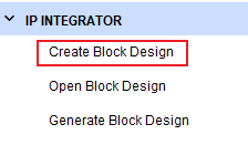
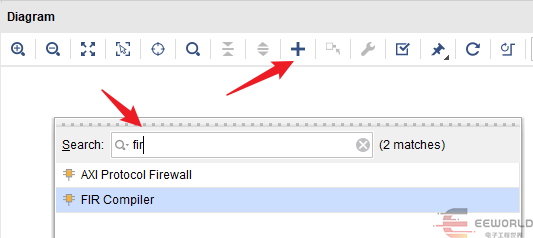
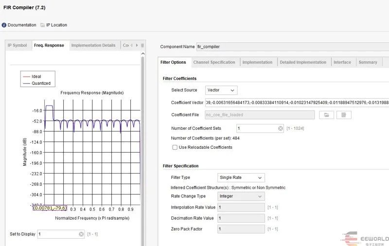
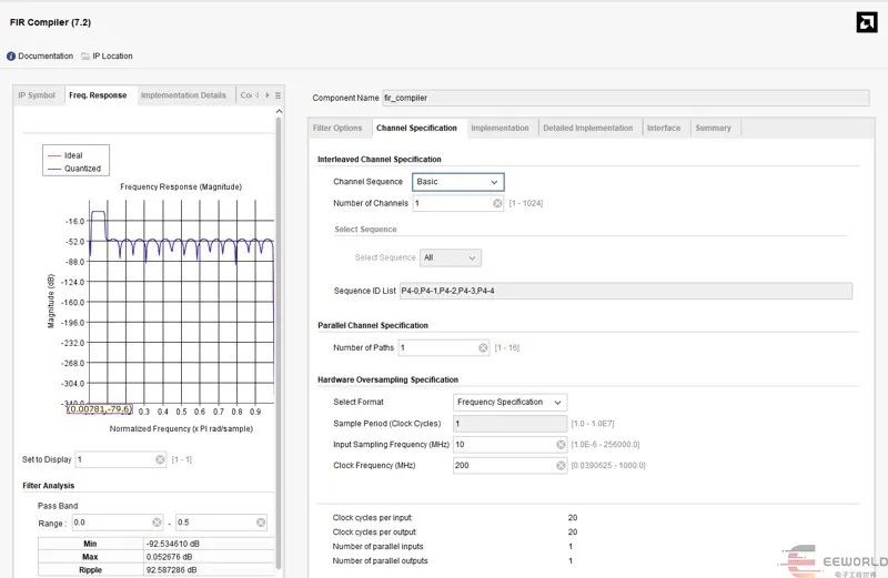
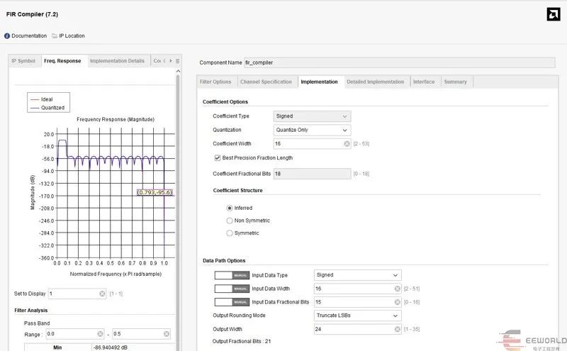
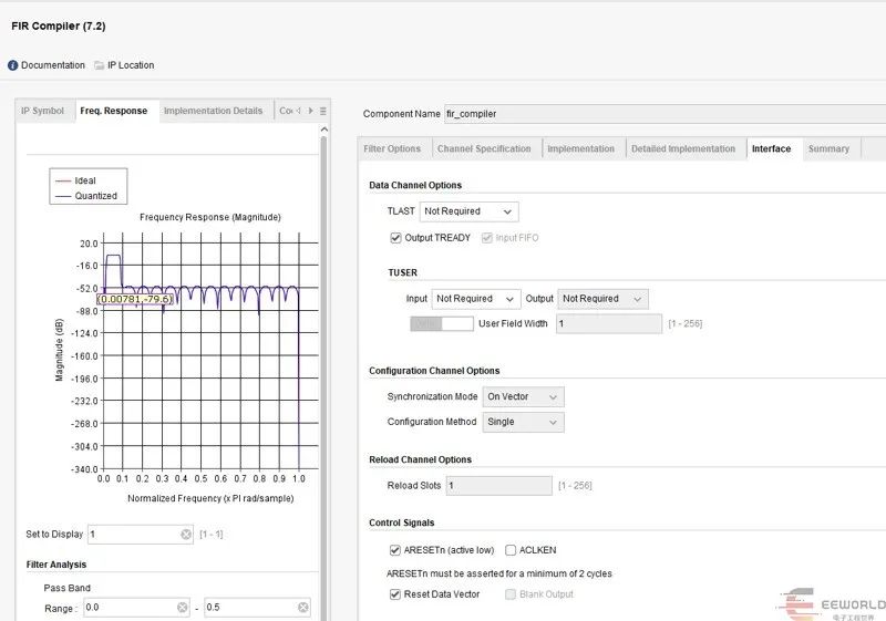
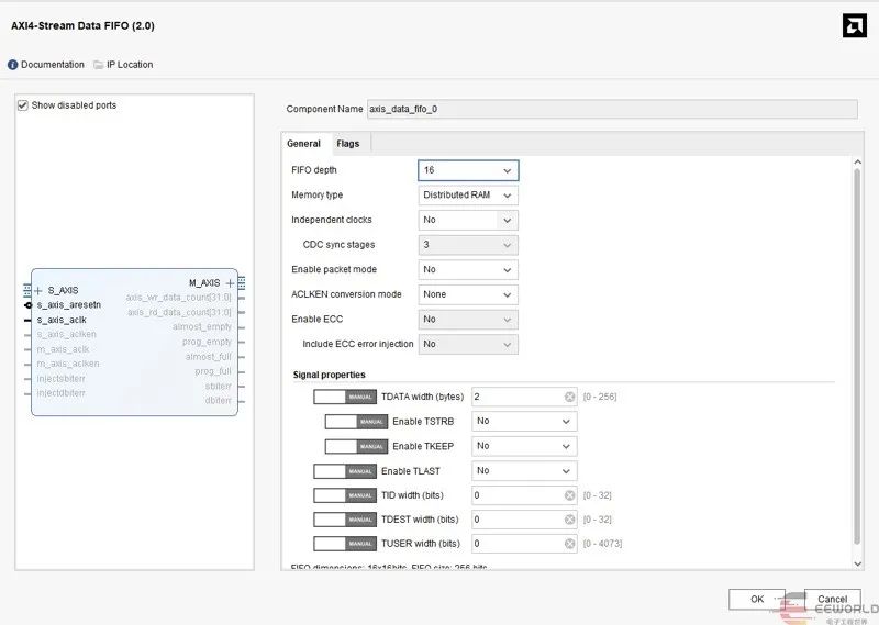
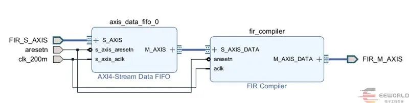
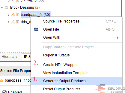
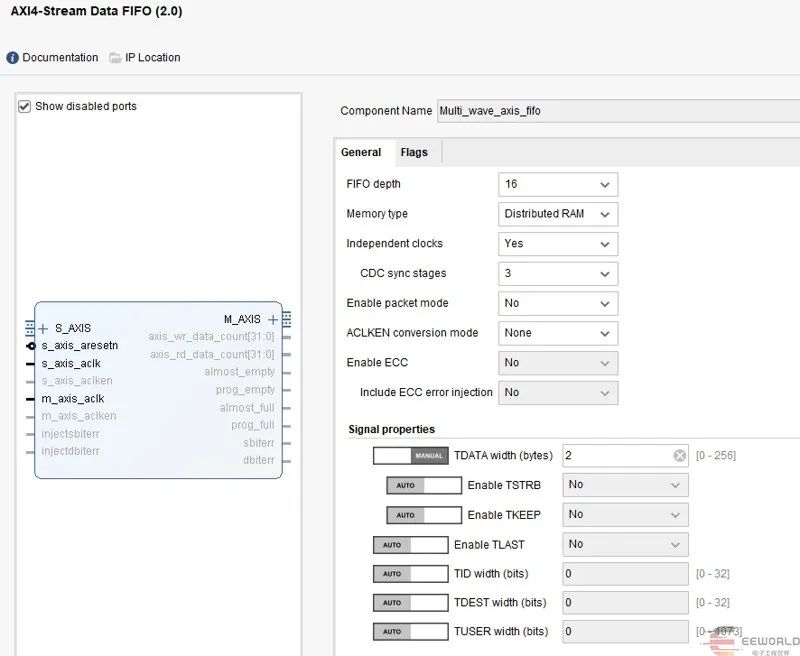
This section skips the process of creating the FPGA project. After creating the project, click on ‘Create Block Design’.Add the FIR IP core.Configure the FIR IP core. In Filter Option, select ‘Vector’ for Select Source, and paste the previously generated coefficients from MATLAB into Coefficient Vector, while keeping the rest as default. You can view the frequency response curve in the left Freq.Response window.In Channel Specification, configure the sampling rate and operating clock. Set input Sampling Frequency (MHz) to 10MHz, and ensure the DDS operating clock matches the sampling rate; configure Clock Frequency (MHz) to 200MHz for the FIR IP core’s operating clock.In the Implement configuration, Coefficient With can be configured as needed. For this design, it is set to 24. By checking the left Freq.Response window, you can see that the red and blue curves closely match the ideal curve, so it is set to 24, but it can be adjusted based on requirements.Configure the Interface as follows:After configuring the FIR, add a fifo with the following configuration:After configuration, connect the FIR and fifo and expose the interface:Finally, right-click on block design, first select ‘generate Output …’ then ‘Create HDL …’.
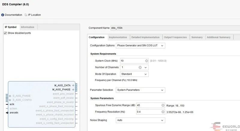
3. Implementing DDS in FPGA
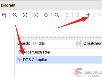
The DDS here is used to generate the input signal for the FIR. Similarly, click on ‘Create Block Design’ and add the DDS IP core.
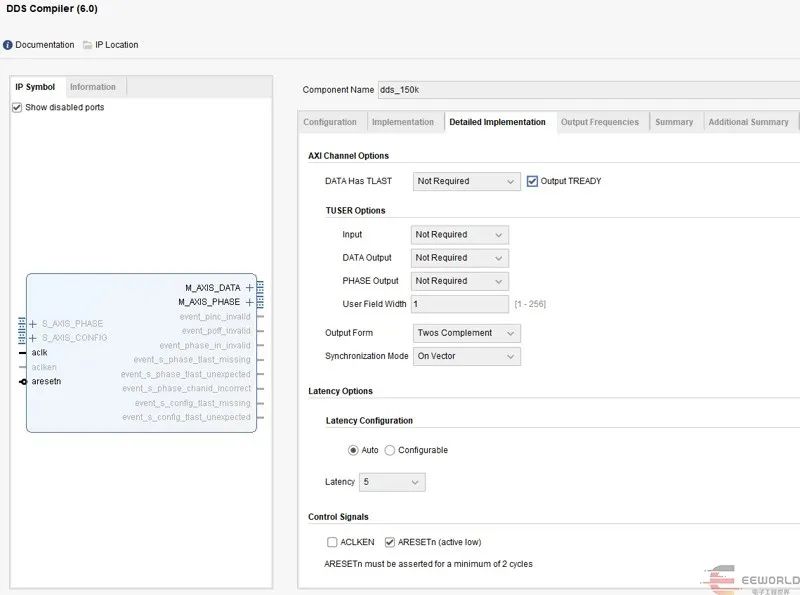
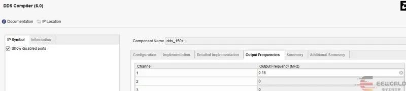
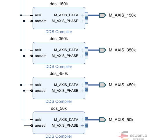
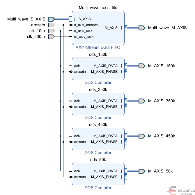
Configure the System Clock (MHz) to 10MHz, keeping the rest of the settings as default.Detailed Implementation configuration is as follows:Finally, configure the output frequency to 0.15MHz or 150kHz, or adjust as needed.Following the above configuration, generate DDS frequencies of 50kHz, 350kHz, and 450kHz.After generating the DDS, create another fifo. This fifo is used to transfer signals generated by the DDS from the 10MHz clock domain to the 200MHz clock domain for FIR filtering. The fifo configuration is as follows: depth 16, data width 16bit.Lastly, connect the generated IP cores as shown in the picture. This DDS is used to test the FIR filter. Externally, you can superimpose the DDS-generated 350kHz and 150kHz signals before inputting them into the fifo. Finally, after crossing the clock domains, output to the FIR for filtering. The superimposed waveform contains the sum frequency (500kHz) and the difference frequency (200kHz). After filtering, only the difference frequency of 200kHz remains. If the filter outputs a 200kHz sine wave, it indicates that the design meets expectations. You can also input single-frequency signals (50kHz/150kHz/350kHz/450kHz) into the filter to observe the output amplitude of the filter.
4. Top Module Implementation
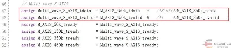
The top module instantiates two block designs. The DDS generates sine signals at 50kHz, 150kHz, 350kHz, and 450kHz. Externally, two of the DDS-generated signals are multiplied and input into the DDS fifo interface, allowing the multiplied signals to cross from the 10MHz clock domain to the 200MHz clock domain, ultimately inputting into the FIR for filtering.If you need to test the FIR filter with a single-frequency signal, you can multiply one of the signals output by the DDS with a constant before inputting it into the FIR for testing.Additionally, the top module should instantiate a PLL to generate a 10MHz clock for the DDS and a 200MHz clock for the FIR.
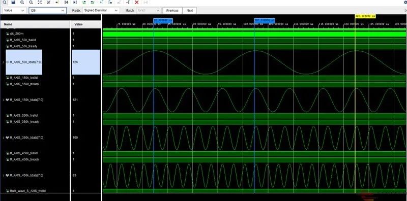
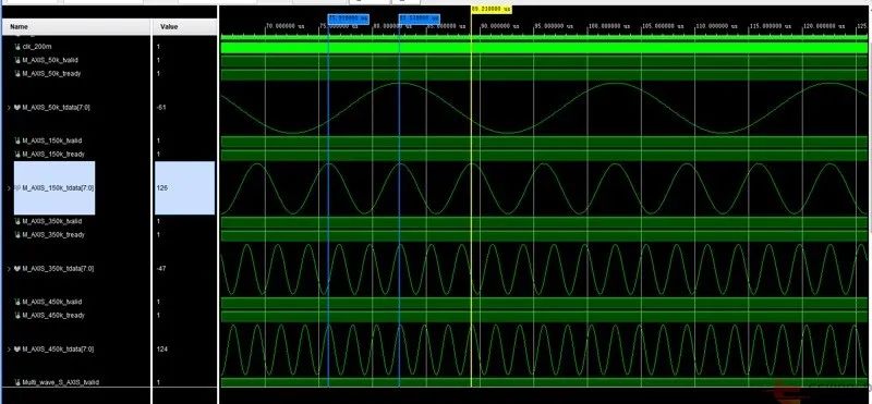
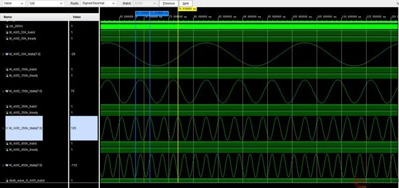
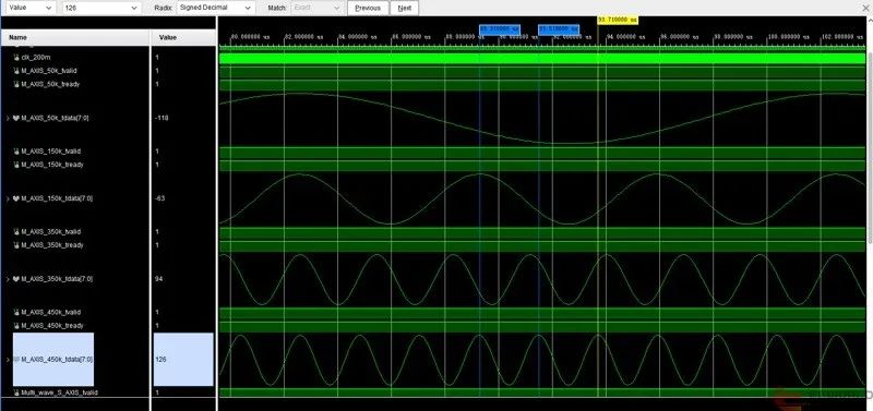
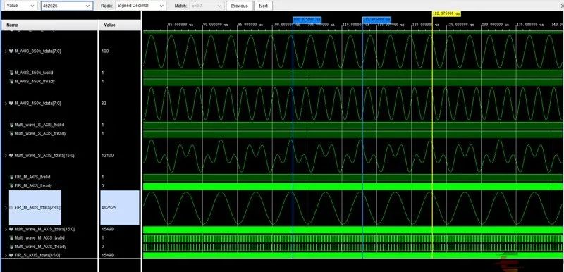
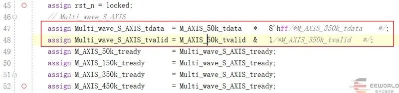
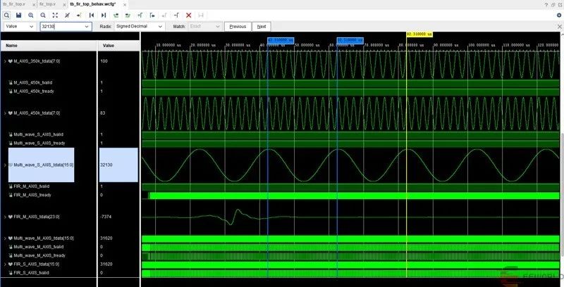
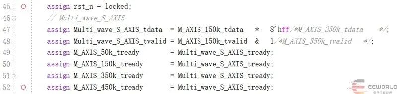
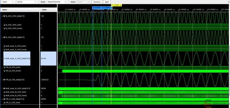
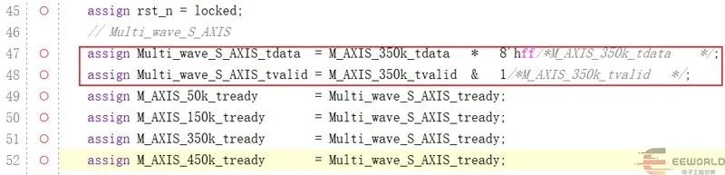
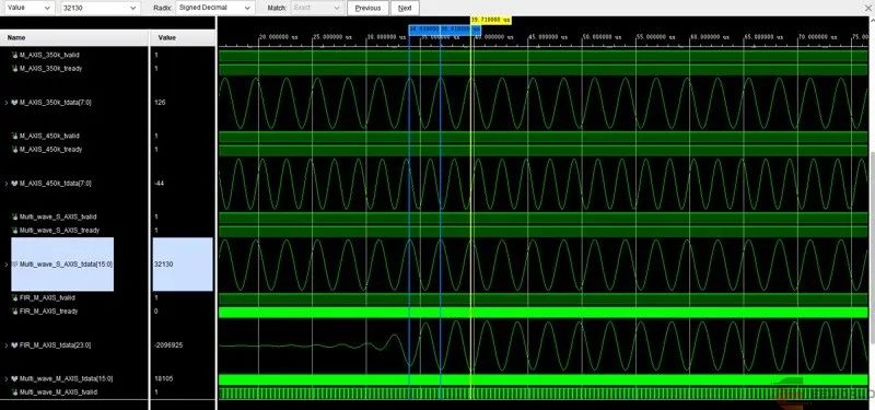
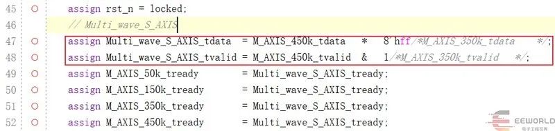
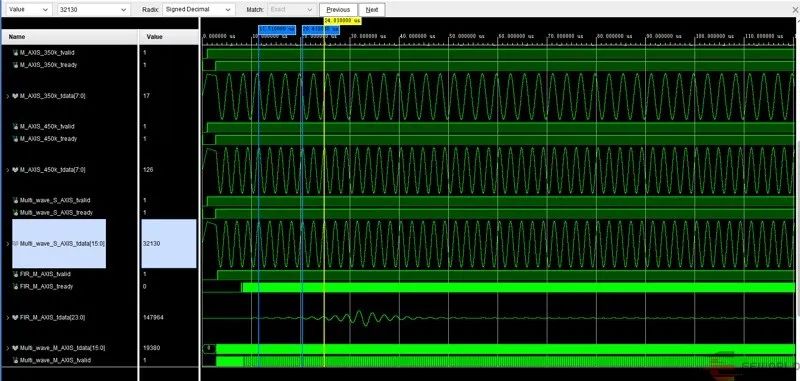
The four signals generated by the DDS are as follows:50kHz signal, with a clock cycle time of 102.31-82.31=20us, which is exactly 50kHz.150kHz, with a clock cycle time of 82.51-75.91=6.6us, frequency approximately 151515Hz.350kHz, with a clock cycle time of 71.21-68.31=2.9us, frequency approximately 344827Hz.450kHz, with a clock cycle time of 91.51-89.31=2.2us, frequency approximately 454545Hz.After superimposing the 150kHz sine wave and the 350kHz sine wave and inputting them into the FIR, the input signal code is modified as follows (the frequency in the image is incorrectly written; the actual signals are 150kHz and 350kHz, while the image shows 450kHz and 350kHz. However, this discrepancy does not affect the FIR testing since the sum and difference frequencies of the two signals are 800kHz and 100kHz. After filtering, the 100kHz signal is output normally while the 800kHz signal is filtered out):The interval between the two cursors is 112.975-102.975=10us, and each clock cycle is 5us, so the frequency of the filter output is 200kHz. Since the input signal is a superposition of a 150kHz sine wave and a 350kHz sine wave, the superimposed waveform contains a sum frequency of 500kHz and a difference frequency of 200kHz. Since 500kHz is outside the passband of the filter, it will be filtered out, leaving only the 200kHz sine wave after filtering. Therefore, the simulation results conform to the filter characteristics. The simulation waveform is shown below, where the FIR_M_AXIS_tdata signal represents the FIR filter output signal.When inputting a 50kHz sine signal into the FIR, the input signal code is modified as follows: the 50kHz signal is superimposed with a constant 8’hff before being input into the FIR.Since 50kHz is outside the filter passband, its amplitude should be attenuated after passing through the filter. The simulation waveform is shown below, where the FIR output signal FIR_M_AXIS_tdata is attenuated, which is consistent with expectations.When inputting a 150kHz sine signal into the FIR, the input signal code is modified as follows: the 150kHz signal is superimposed with a constant 8’hff before being input into the FIR.Since 150kHz is within the filter passband, its amplitude remains unchanged after passing through the filter. The simulation waveform is shown below, where the FIR output signal FIR_M_AXIS_tdata maintains its amplitude, which is consistent with expectations.When inputting a 350kHz sine signal into the FIR, the input signal code is modified as follows: the 350kHz signal is superimposed with a constant 8’hff before being input into the FIR.Since 350kHz is within the filter passband, its amplitude remains unchanged after passing through the filter. The simulation waveform is shown below, where the FIR output signal FIR_M_AXIS_tdata maintains its amplitude, which is consistent with expectations.When inputting a 450kHz sine signal into the FIR, the input signal code is modified as follows: the 450kHz signal is superimposed with a constant 8’hff before being input into the FIR.Since 450kHz is outside the filter passband, its amplitude should be attenuated after passing through the filter. The simulation waveform is shown below, where the FIR output signal FIR_M_AXIS_tdata is attenuated, which is consistent with expectations.
6. Conclusion
From the simulation results, it can be seen that whether the input signal is a single frequency signal or a superimposed dual frequency signal, the results meet expectations. For the source code of the related project, please click Read Original, to download in the original post.
· END ·
Welcome to mark us as “Starred” so you can receive push notifications promptly.
Follow the “Automotive Development Circle” below and reply “Auto” to receive a free Autosar introductory and practical materials package!
Scan to add the assistant and reply “Join Group”
Communicate experiences face-to-face with electronic engineers