The author has summarized the I2C specifications into one article, with the following table of contents:
I2C Introduction
I2C Architecture
I2C Transfer
I2C Synchronization And Arbitration
I2C Hs-mode
1. I2C Introduction
1.1 I2C History
-
I2C: Inter-Integrated Circuit, an integrated circuit bus. -
I2C is a simple, bidirectional two-wire synchronous serial bus designed by Philips in 1982 for motherboards and embedded systems (short distance). -
Philips Semiconductor Division is now NXP. -
The patent for I2C expired on November 1, 2006, and is free for everyone to use. -
The I2C-compatible bus (System Management Bus) introduced by Intel in 1995, known as SMBus or SMB. -
The latest version of the I2C specification v.6 was released on April 4, 2014.
1.2 Future of I2C
-
The MIPI Alliance finalized the I3C (improved Inter-Integrated Circuit) specification around 2014, which builds a superset of features on the I2C specification, supporting high-speed transmission modes. -
Currently, both SoC manufacturers and device manufacturers have begun or are transitioning to I3C. -
The I3C specification has versions from 2016, 2018, and the latest is from 2021 (446 pages).
1.3 Speed of I2C
-
Pronunciation of I2C: “I squared C”, “I two C”. -
I2C is a low-speed serial bus with SDA (Serial Data Line) and SCL (Serial Clock Line) as the two signal lines, operating in half-duplex communication.
Communication speeds are as follows:
• Bidirectional bus:
-
Standard-mode (Sm), 100 kbit/s -
Fast-mode (Fm), 400 kbit/s, used in sensors, cameras, touch, etc. -
Fast-mode Plus (Fm+), 1 Mbit/s -
High-speed mode (Hs-mode), 3.4 Mbit/s, used in NFC, buck & boost, etc.
• Unidirectional bus:
-
Ultra Fast-mode (UFm), 5 Mbit/s
The speed is determined by SCL, and different modes have different requirements for the rising edge, which is influenced by pull-up resistors and equivalent capacitance.
1.4 I2C as a Multi-Master/Slave Architecture Bus
-
I2C read/write is initiated by the master side. -
Every byte (8 bits) of I2C communication requires an ACK/NACK response from the slave side. -
Multiple master sides require an arbitration mechanism. -
The slave side is distinguished by device addresses, which can be 7 bits or 10 bits, and there is also an 8-bit address, which is actually 7 bits + read/write bit. [The 7-bit address = type number (4 bits) + address code (3 bits)]
1.5 How Many Devices Can Be Connected to the I2C Bus?
7-bit address: 2 to the power of 7, can connect 128 devices.
10-bit address: 2 to the power of 10, can connect 1024 devices.
However, the I2C protocol stipulates that the capacitance on the bus cannot exceed 400pF. Pins have input capacitance, and the PCB will also have parasitic capacitance, so there is a limit. In practical design, the empirical value is generally no more than 8 devices.
The reason for the capacitance limit on the bus is that the GPIO used by I2C is generally an open-drain structure, requiring external pull-up resistors. The resistor and bus capacitance create an RC delay effect; the larger the capacitance, the slower the signal edges, which may lead to signal quality risks (square wave turning into triangle wave). The faster the transmission speed, the smaller the signal window, and the rise and fall time requirements become shorter and steeper, so the RC product must be smaller. (It can be understood that outputting a high level is charging the capacitor; the larger the capacitor, the slower the charging.)
Note: Remove the reserved device addresses specified by the spec, keeping the following addresses:
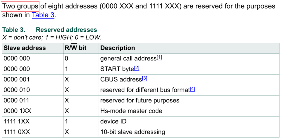
Note: It is written as two groups, not just eight, the 0000 XXX and 1111 XXX series addresses are reserved.
Note: Be aware that 1111 1XXX is the Hs-mode master code, and 1111 0XXX is for 10-bit slave addressing, which the author will discuss later.
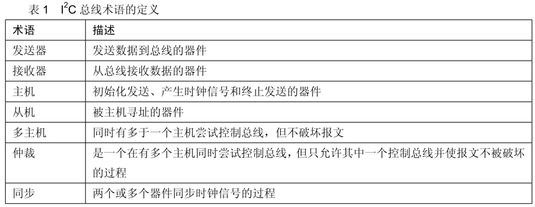
1.6 Terminology Definitions
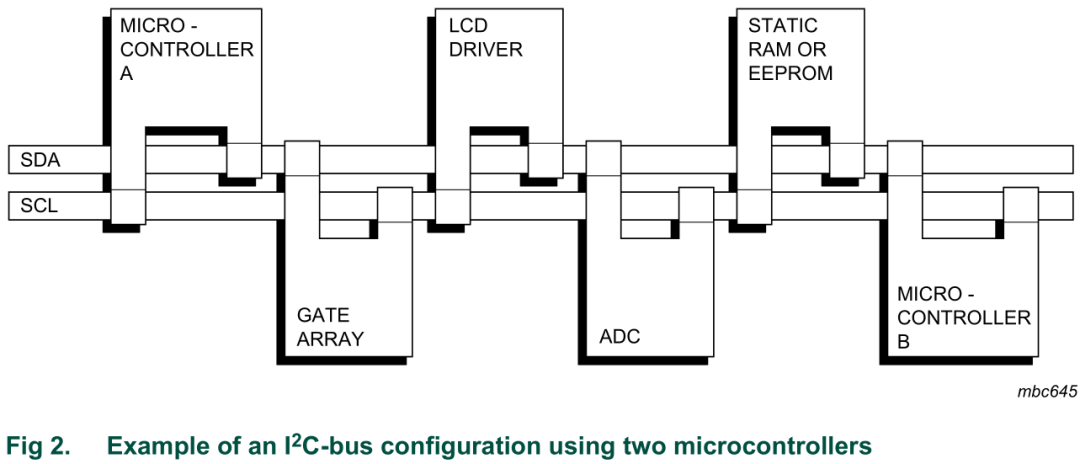
2. I2C Architecture
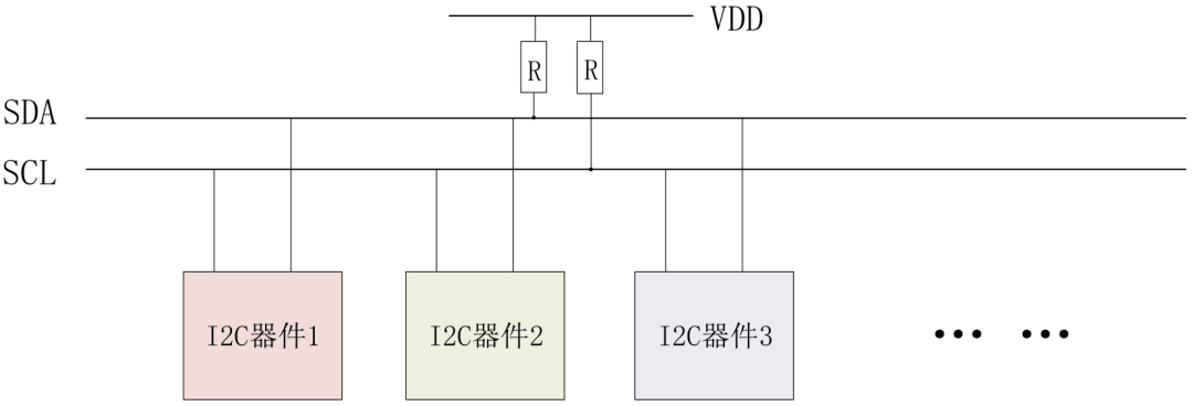
I2C uses GPIO that is generally in an open-drain mode, supporting wired-AND functionality. However, the open-drain mode cannot output a high level, so external pull-ups are required. Vdd can be 5V, 3.3V, 1.8V, etc., and the pull-up resistor values differ with power supply voltage.
It is generally considered that on the I2C bus, below 0.3Vdd is low, and above 0.7Vdd is high.
Each device connected to the bus has a unique static device address.
When idle, both lines on the I2C bus are high due to the pull-up resistors.
2.1 Push-Pull and Open-Drain Structures
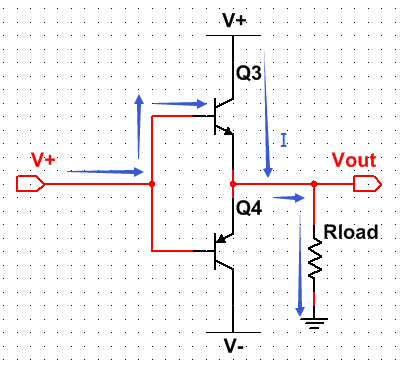
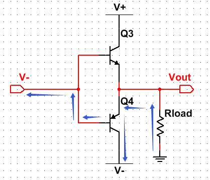
1. Push-pull structure: uses two transistors or MOSFETs, existing in the circuit in a push-pull manner. During operation, only one of the two symmetrical switch tubes is conducting, resulting in low conduction loss and high efficiency. It can both sink current to the load and source current from the load. The push-pull output stage enhances the circuit’s load capacity and increases switching speed.
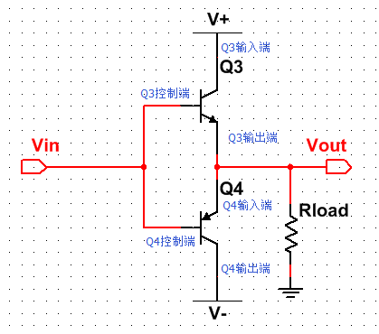
The figure shows an NPN transistor on top and a PNP transistor below. There are two cases:
Output high level: sourcing current to the load.
Output low level: sinking current from the load.
2. Open-drain structure (OD): In contrast to the push-pull structure, the open-drain structure has only one transistor or MOSFET.
The reason it is called open-drain is that the MOSFET has three terminals: source, gate, and drain. The drain is open-circuit output, hence the name open-drain; if it is a transistor: base, collector, and emitter, the collector is open-circuit output, thus called open-collector (OC).
Open-collector output, NPN transistor:
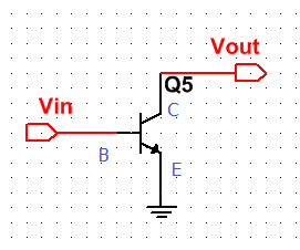
When Vin is high, the transistor conducts, outputting low level externally, pulling the line low directly.
When Vin is low, the collector (C) is open-circuit, and the output level state is determined by external factors.
The above analysis uses a transistor, but MOSFETs are similar.
Thus, the push-pull structure can output both high and low levels. The open-drain output can only output low levels, with the high level determined by external circuitry.
2.2 Wired-AND Functionality
Wired-AND: All GPIOs output high, the entire line is high; as long as one outputs low, the entire line is low, this is the meaning of “AND”.
1. In a push-pull structure, if two GPIOs are connected to one line, if the left PMOS is conducting and the right NMOS is conducting, Vdd will be directly grounded through both MOSFETs. Since the conduction resistance of the MOSFETs is low, this can lead to a large current, potentially damaging both GPIOs; therefore, push-pull output does not support wired-AND.
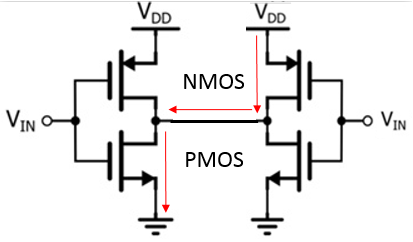
Note: It is not necessarily the above NMOS below PMOS; as long as the two transistors are of different types, only one can conduct at a time, allowing both high and low levels to be output.
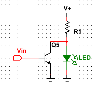
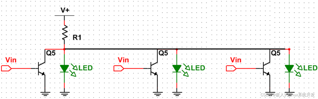
2. In an open-drain structure, if many GPIOs are open-drain and connected to one line, as shown in the figure below. The high level output of the open-drain structure relies on external pull-up. If one GPIO is grounded, the current will flow through the pull-up resistor to ground. Because of the presence of the pull-up resistor, the current is not large, and GPIO will not be damaged.
Wired-AND is the foundation of the I2C protocol!
Summary
| Mode | Open-Drain | Push-Pull |
|---|---|---|
| Speed | Slower | Faster |
| Power | Higher | Lower |
| Slave Clock Stretching | Yes | Not Supported |
In terms of power consumption, the open-drain structure consumes more energy due to the pull-up resistor during each high-low level transition.
Regarding clock stretching, the open-drain supports clock stretching, while the push-pull structure does not. The reason is similar to why push-pull does not support wired-AND. Some may wonder, isn’t clock stretching when the slave pulls the SCL line low? It shouldn’t be a problem. However, if it is a push-pull GPIO, the master will attempt to pull the SCL high, only to find it pulled low by the slave, which would cause a short circuit.
Again, to remind, wired-AND: as long as one device on the bus outputs a low level, the entire bus is in a low state, and the bus is considered occupied.
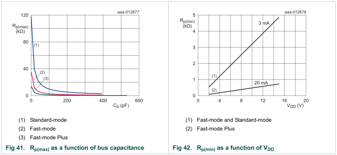
2.3 Pull-Up Resistor Calculation
1. If the pull-up resistor is too small, the current will be large, causing the port low level to rise, and the voltage on the bus may not reach 0V.
2. If the pull-up resistor is too large, the rise time will increase, and the square wave may turn into a triangle wave.
Thus, calculating an accurate pull-up resistor value is very important. The calculation of pull-up resistor values has a clear formula:
Maximum resistance is related to rise time tr, bus capacitance Cb, and standard rise time 0.8473.
Minimum resistance is related to power supply Vdd voltage, GPIO maximum output voltage Vol, and GPIO maximum current Vol.
Refer to section 7.1 of the “I2C-bus specification and user manual.pdf”: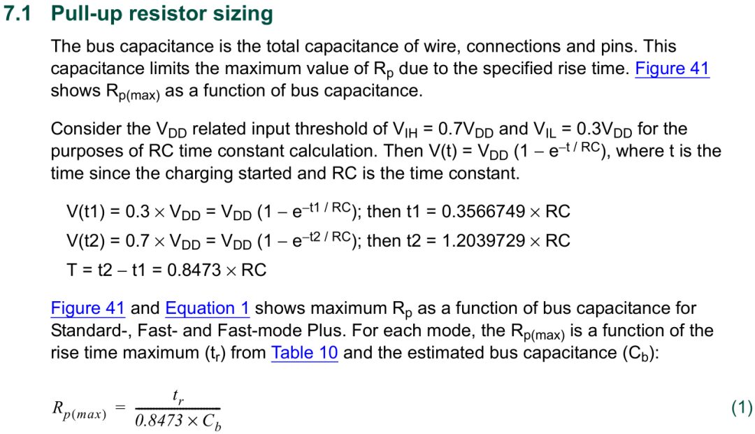
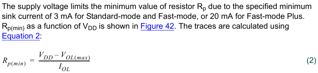
Refer to Table 10 in the “I2C-bus specification and user manual.pdf”:
From the above figure, we can derive the calculation formulas for maximum and minimum resistances as well as the following data:
1. Standard mode: 0~100KHz, rise time requirement tr = 1us
2. Fast mode: 100~400KHz, rise time requirement tr = 0.3us
3. High-speed mode: up to 3.4MHz, rise time requirement tr = 0.12us
Note: The rise time tr is the time requirement from 0.3Vdd to 0.7Vdd.
Assuming: Vdd is 1.8V, Cb bus capacitance is 200pF (Although the protocol specifies a maximum load capacitance of 400pF, in practice, the waveform becomes poor beyond 200pF; we calculate with 200pF, and it is recommended to use 100pF in practice).
Standard mode:

Fast mode:

High-speed mode:

Minimum resistance (the larger the Vdd, the larger the pull-up resistor):

Note: In high-speed mode, the power supply voltage is generally 1.8V, not 3.3V, because if calculated with 3.3V, you will find the minimum resistance larger than the maximum resistance.
Using appropriate power supply voltage and appropriate pull-up resistor will optimize your I2C transmission signal.
Common resistor values used at different speeds include: 1.5K, 2.2K, 4.7K.
Pull-Up Resistor Relationship Diagram

3. I2C Transfer
3.0 Definition of Timing
To deeply explore the I2C protocol, it is essential to understand the definitions of various timings, as follows for F/S-mode:
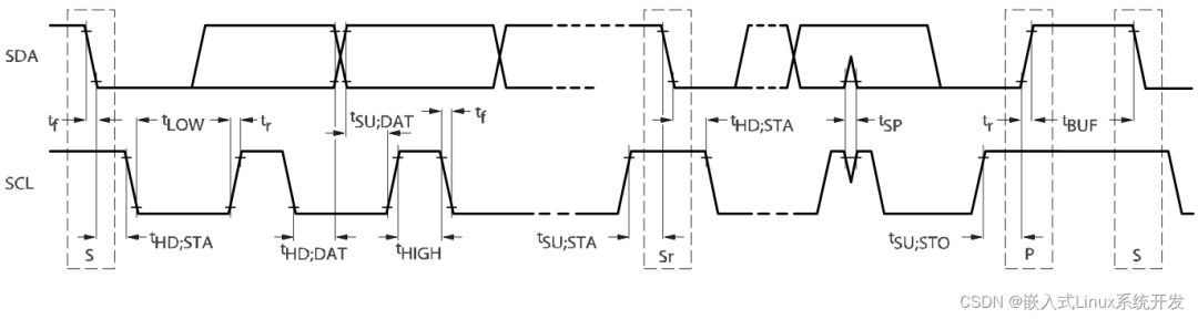
-
Setup time (Tsu): The time interval before the clock rising edge when the input data has arrived and remains stable. -
Hold time (Thd): The time interval after the clock rising edge during which the input data remains stable.
| Identifier | Definition |
|---|---|
| tf | Signal falling time |
| tr | Signal rising time |
| tLOW | Signal low level time |
| tHIGH | Signal high level time |
| tHD;DAT | Data hold time |
| tSU;DAT | Data setup time |
| tSP | Input filter must suppress the pulse width |
| tBUF | Idle time for start and stop conditions |
| tHD;STA | Hold time for repeated start condition |
| tSU;STA | Setup time for repeated start condition |
| tSU;STO | Stop condition setup time |
Sr is repeated start, S is start, P is stop.
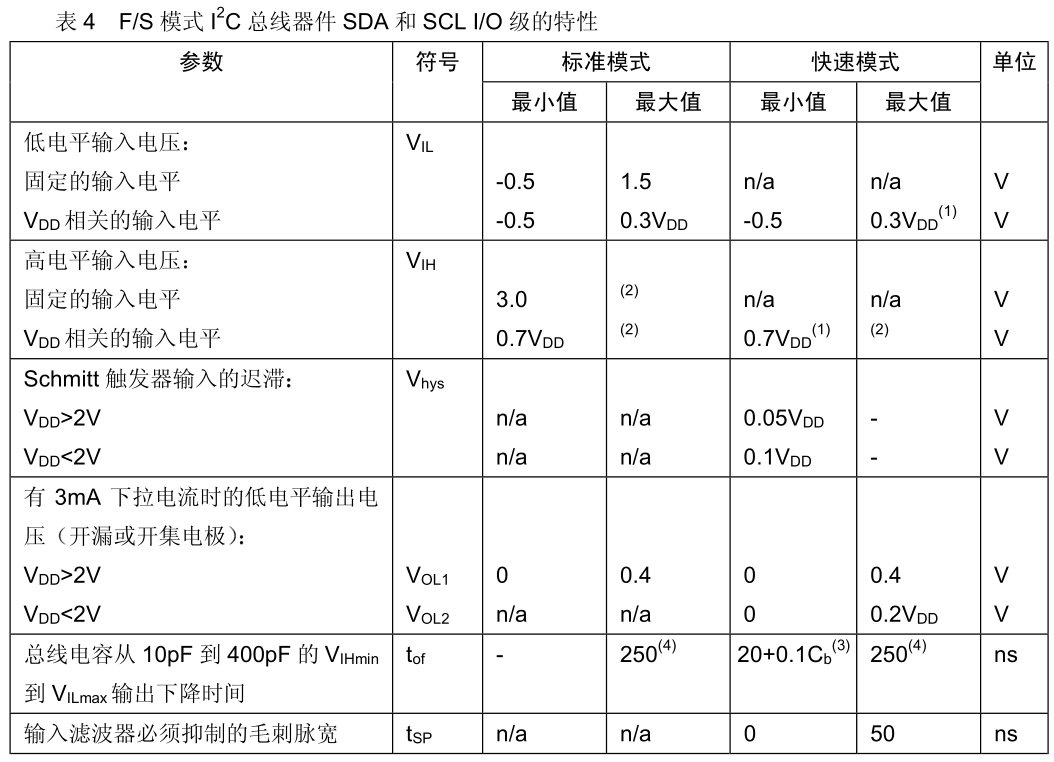
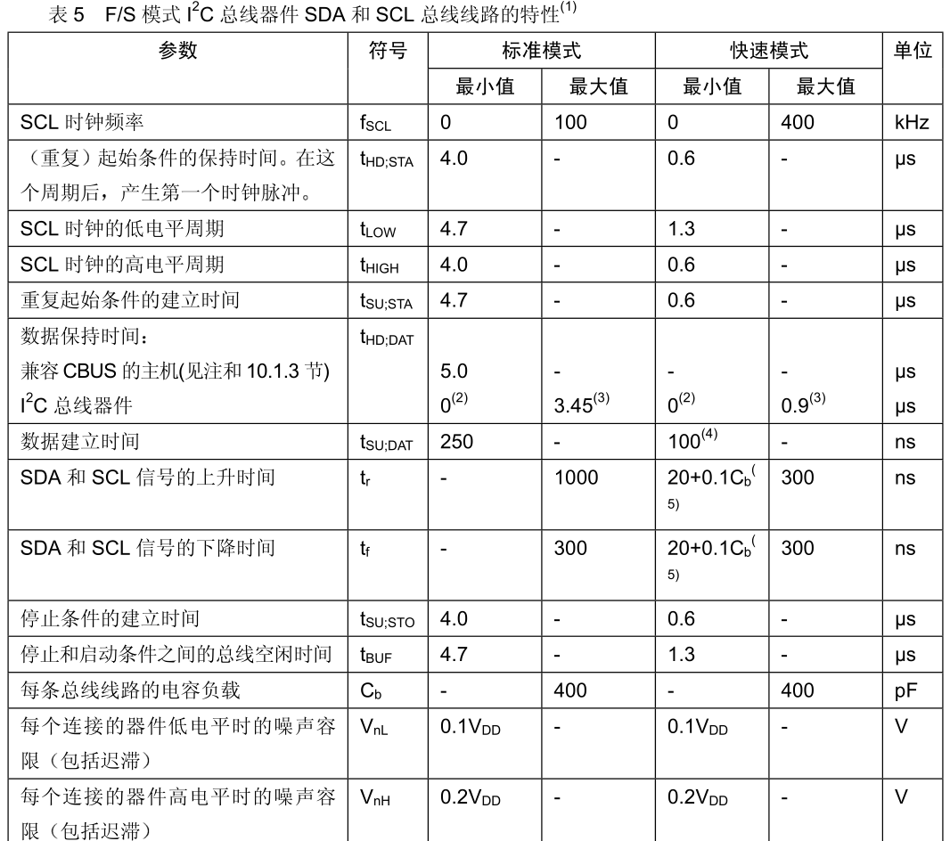
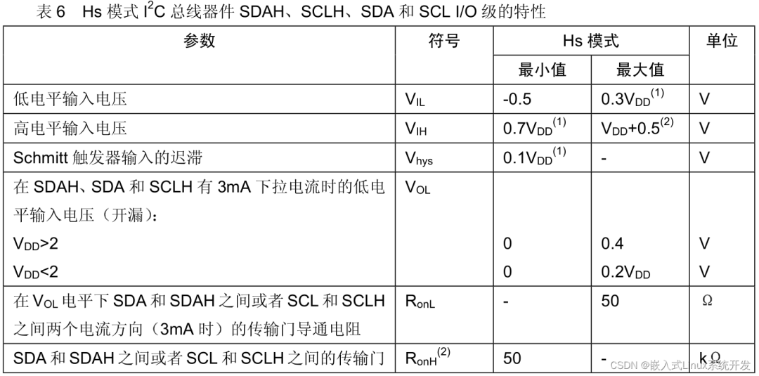
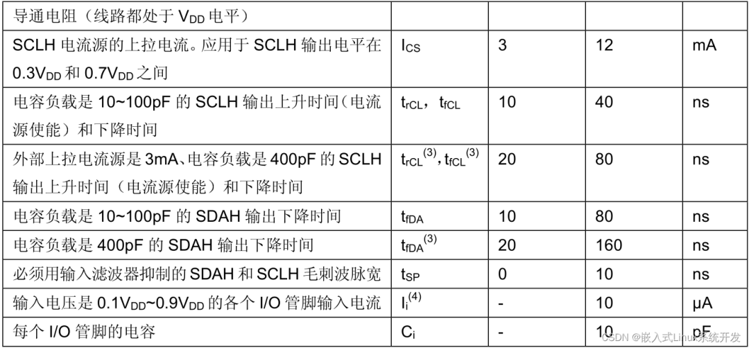
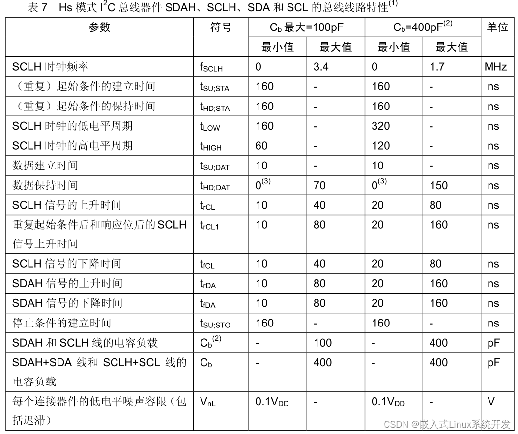
The above parameters are strictly specified in the spec, and can be found in tables; generally, standard mode and fast mode are combined, while Hs mode is listed separately, in Tables 4, 5, 6, and 7:

Master
-
Provides clock SCL -
Initiates and terminates data transmission -
Addresses other devices
Slave
-
Addressed by the master device
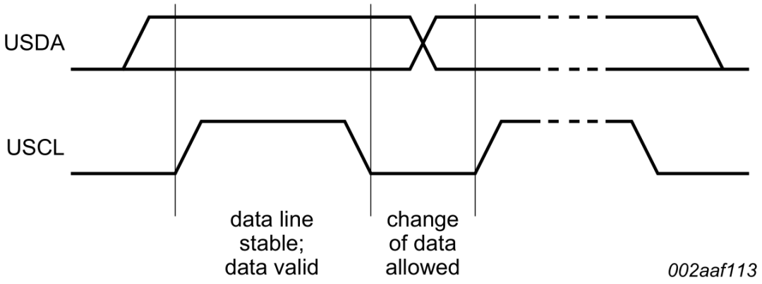
3.1 Data Validity
During SCL high, SDA must be stable, so generally, SCL high width is small, and SDA high width is large, which is also visible on an oscilloscope.
3.2 Start and Stop Conditions
Start condition: SDA goes from high to low while SCL is high.
Stop condition: SDA goes from low to high while SCL is high.
Note: Because SCL and SDA lines have pull-up resistors, both lines are high when idle. Therefore, the START condition must pull one line low; the spec specifies that the SDA line must be pulled low for the start condition. This is also the reason why start and stop conditions cannot be interchanged (the reason why SCL cannot be pulled low for the start condition will be understood later).
Byte Format
-
The transmission length must be one byte (8 bits) -
The number of bytes transmitted at a time is not limited -
Data must be transmitted starting from MSB, meaning the highest bit is transmitted first -
The slave can hold the clock line SCL low, forcing the master into a wait state. 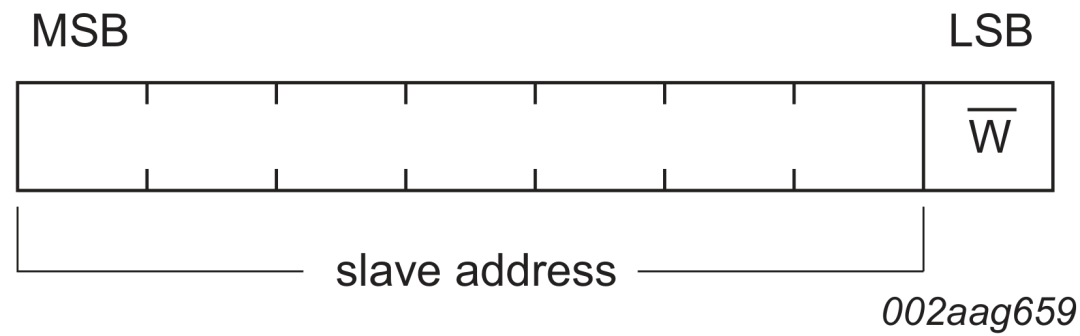
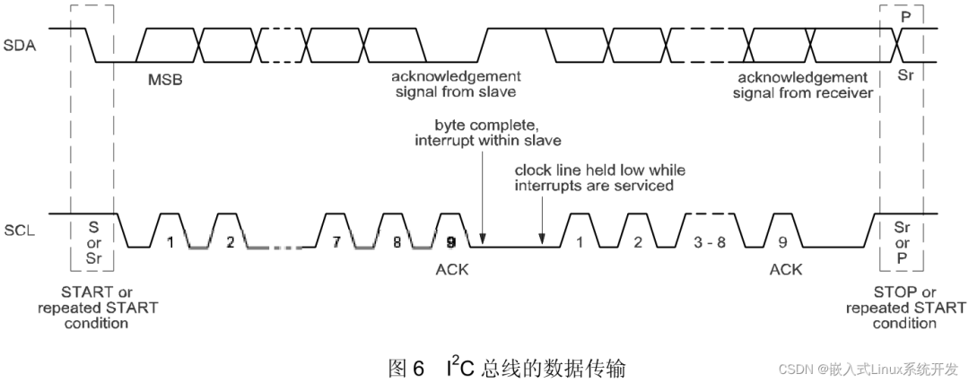
After ACK, the slave can pull the SCL line low for clock stretching (for example, if the slave needs to prepare data, etc.).
Note: While SCL is high, SDA is sampled; if SDA is high, it is 1; if low, it is 0. During SCL low, SDA can change data. It is not allowed to change data while SCL is high, or it will be considered a start and stop condition.
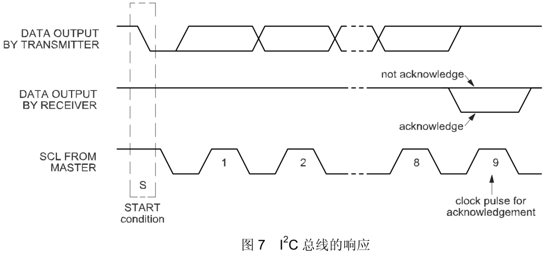
3.3 ACK or NACK
After transmitting one byte, the slave must respond with either ACK or NACK.
ACK: After transmitting 8 bits, on the ninth bit, if SCL is high and SDA is low, it indicates an ACK response.
NACK: After transmitting 8 bits, on the ninth bit, if SCL is high and SDA is high, it indicates a NACK response.

The spec specifies five situations where NACK may occur:
-
The master sends an address on the bus that does not match any slave, resulting in NACK. -
The slave is busy, resulting in NACK. -
During transmission, the slave receives data or commands it does not understand. -
During transmission, the slave can no longer receive any data bytes. -
When the master receiver must send a signal to the slave transmitter to end the transmission, NACK will occur.
3.4 Write Data
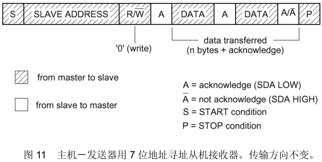 The master writes data to the slave; at the last byte of communication, normally the slave will respond with an ACK, indicating the last byte was written successfully, after which the master will generate a STOP signal.
If the last byte receives a NACK from the slave, the master will also generate a STOP signal and report an ACK error to the upper layer.
How the upper layer handles it is the upper layer’s business; during chip design, the I2C peripheral controller will generate an ACK error at this time. If using a Linux operating system, it can be configured to ignore this last ACK error at the upper layer.
3.5 Read Data
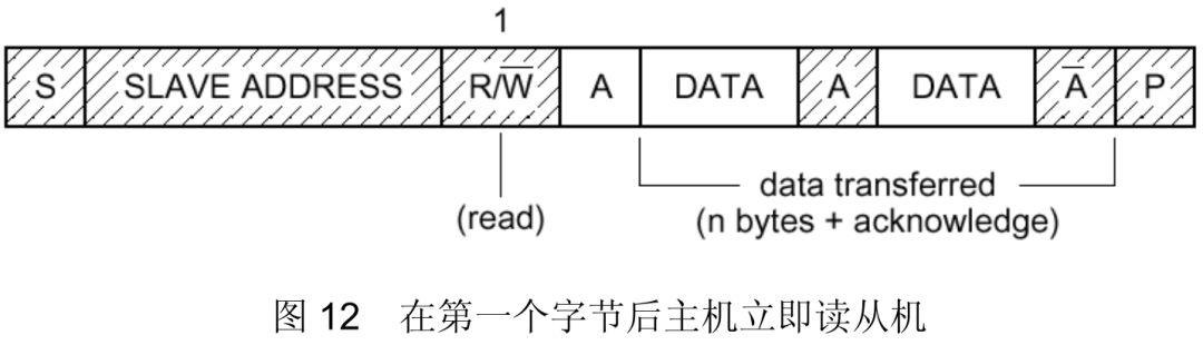 The master reads data from the slave; after the last byte, the master will send a NACK to the slave, indicating no further data will be read, followed by the master generating a STOP signal. This is the only NACK during the normal transmission process.
3.6 Composite Format
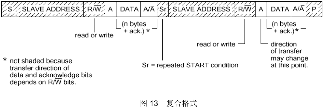 In the repeated start signal (Sr), the two slave addresses can be different. This means that one I2C master can issue a repeated start signal to access another slave without generating a STOP signal. (If there are multiple masters on the I2C bus, no arbitration is needed again, saving time).
Additionally, in the Linux system, due to the specification of the i2c_msg structure, the maximum single I2C transmission is 64KB; exceeding this requires a STOP signal or repeated start signal.
3.7 I2C Transfer Regulation
-
Starts with the START condition -
Ends with the STOP condition -
The first byte transmitted is the 7-bit slave address + 1-bit read/write bit -
Each device on the bus compares the 7-bit address following the START signal with its own address for a match -
Each byte (8 bits) will have an ACK or NACK following it -
After the START or repeated START signal, the slave must reset its bus logic -
A START followed immediately by a STOP signal is an illegal format -
The master can skip generating a STOP signal and instead generate a repeated START signal + address of another device to begin accessing another device
3.8 10-Bit Addressing
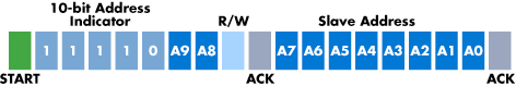
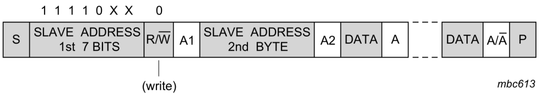
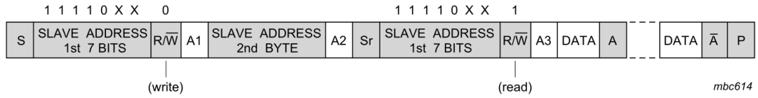
The 10-bit slave address is defined as follows, where 11110 indicates a 10-bit address, and A9-A0 represents the 10 bits address:
The master writes data to the slave (requires 2 bytes)
The master reads data from the slave (requires 3 bytes)
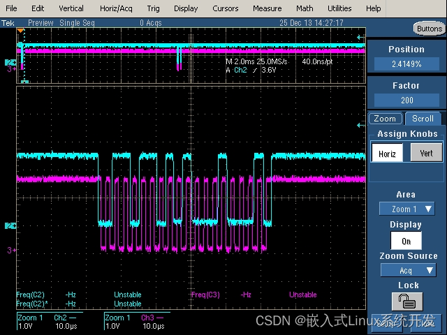
3.9 Oscilloscope Waveform Example
-
The master writes data to the slave
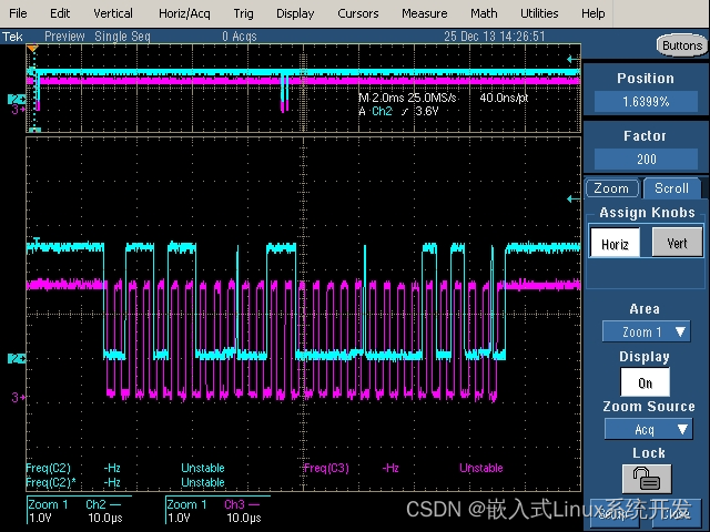
In the above figure, you will find three very thin glitches on the SDA line, which occur every time the slave responds with an ACK. This is due to the slave pulling the SDA line low to respond with ACK, then releasing the SDA line, which is pulled high by the pull-up resistor, and then the master immediately takes over the SDA line and pulls it low. Thus, this glitch is caused by the timing difference between the slave and master handover.
Because this glitch occurs during SCL low, and during SCL low, SDA can change data, it does not negatively impact I2C communication, and this glitch is generally not a concern.
If you find the waveform unsightly, you can consult the chip manufacturer to see if the master control line’s setup time and hold time can be adjusted to reduce the amplitude of this glitch.
-
The master reads data from the slave
3.10 Supplement
I2C does not support slaves initiating an interrupt on the SCL and SDA lines to notify the master to read data. Slaves needing an interrupt must connect an additional interrupt line to notify the master that data is ready, prompting the master to initiate a read operation.
This undoubtedly increases system complexity and occupies more pins. I3C does not have this issue; I3C allows slaves to initiate interrupts on the SCL and SDA lines, called “in-band interrupts”, which will be discussed later.
4. I2C Synchronization And Arbitration
Three concepts: clock stretching, synchronization, arbitration
4.1 Clock Stretching
-
Clock stretching: Pausing transmission by holding the SCL line low. Transmission cannot proceed until SCL is pulled high again. -
The slave can pull the SCL line low, forcing the master into a wait state. -
Clock stretching is optional and not mandatory.
Byte Level
Clock stretching requires more time to store the received byte or prepare another byte for transmission.
Bit Level
By extending each clock low period, the total bus clock is reduced. The speed of any master is adapted to the internal operating speed of that device.
In Hs mode, only byte level can be used, meaning clock stretching can only be done after one byte (8 bits) is transmitted. In Standard-mode and Fast-mode, both byte level and bit level can be used; bit level means that even if you only transmit 2 bits, the slave can pull the SCL line low for clock stretching, temporarily pausing transmission.
Clock Stretching Simplified Explanation
The I2C master always controls the clock line SCL, whether writing to a device or reading from it. Generally, if the target is an EEPROM or other simple device, it doesn’t matter, but if the slave is a processor that needs to perform some calculations after receiving a command from the master and then return the results, it may not be able to keep up. What to do? At this point, the slave will actively control the clock line, pulling it low until the data is ready, then releasing the clock line and handing control back to the master. This is the only moment the slave can control the bus in the I2C communication system!
The key is that many I2C masters do not support the clock stretching feature, making it impossible to communicate with slaves that have clock stretching capabilities! Therefore, when selecting master components, you must pay attention to this; otherwise, the entire design may fail, causing significant impact.
4.2 Synchronization And Arbitration
I2C is a multi-master/slave architecture, meaning multiple I2C masters and multiple I2C slaves can be connected to a single bus simultaneously.
However, if two or more masters simultaneously send a start signal to the bus and begin transmitting data, a conflict will arise. To resolve this conflict, arbitration must occur, which is the arbitration on the I2C bus.
Arbitration on the I2C bus consists of two parts: SCL line synchronization and SDA line arbitration; these two parts occur simultaneously without a specific order.
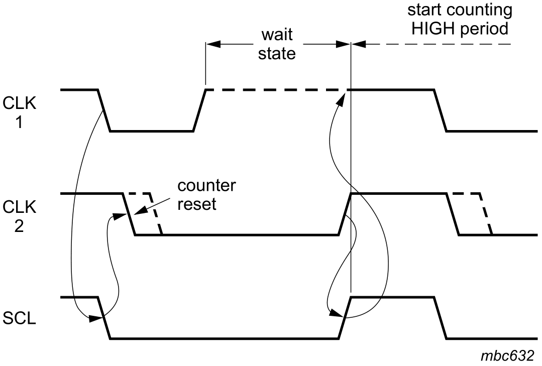
4.3 SCL Synchronization
All masters output their clock on the SCL line, thus the synchronization process requires defining their own clock.
SCL synchronization occurs due to the bus’s wired-AND logic functionality, meaning that as long as one node sends a low level, the bus will exhibit a low level. The bus can only show a high level when all nodes send high levels. It is precisely due to the wired-AND logic function that when multiple nodes send clock signals simultaneously, the bus exhibits a unified clock signal. This is the synchronization principle of SCL.
The synchronization process is illustrated below:
Master 1 generates CLK1, and Master 2 generates CLK2, both outputting their clocks to the SCL line. Because CLK2 has a longer low level, the SCL line reflects the level of CLK2. Thus, during the first cycle, CLK1 enters a high level wait state. The subsequent SCL levels will follow CLK2.
4.4 SDA Arbitration
SDA line arbitration is also based on the principle of the bus’s wired-AND logic functionality. After sending one bit of data, nodes compare the data presented on the bus with what they sent. If they match, they continue sending; if not, they exit the competition.
SDA line arbitration ensures that the I2C bus system can communicate normally and not lose data when multiple master nodes attempt to control the bus simultaneously. The bus system allows only one master node to continue occupying the bus through arbitration.
-
Arbitration occurs on SDA, while SCL is high. -
Master A transmits high, Master B transmits low, Master A loses arbitration. -
The master that loses arbitration will generate clock pulses until the byte in which arbitration was lost ends.
Arbitration Process:
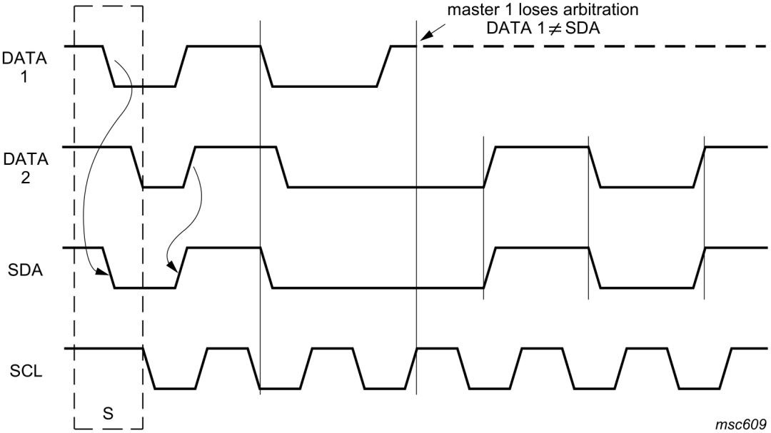
DATA1 and DATA2 are the data signals sent to the bus by two masters; SDA is the data signal presented on the bus, and SCL is the clock signal presented on the bus.
Master 1 and 2 simultaneously send start signals; during clock 1, both masters send high signals. The bus shows a high signal, and both master nodes detect that the bus signal matches their sent signal, so they continue sending data.
In the second clock cycle, both master nodes send low signals, and the bus shows a low signal, continuing to send data.
In the third clock cycle, master node 1 sends a high signal while master node 2 sends a low signal. Due to the wired-AND logic function, the bus signal is low, and master node 1 detects that the bus data does not match what it sent, so it disconnects the data output stage and switches to slave receiving mode. Thus, master node 2 wins the bus, and the data is not lost, meaning the bus data matches what master node 2 sent. Master node 1, after turning into a slave node, continues to receive data, also without losing data on the SDA line. Therefore, no data is lost during the arbitration process.
5. I2C Hs-mode
Why is HS mode discussed separately? Because high-speed mode has many differences from other modes.
-
Speed up to 3.4MHz. -
Uses SDAH and SCLH signal lines, not SDA and SCL.
Master Device
-
SDAH/SCLH has an open-drain output buffer, and SCLH has a current source pull-up circuit that shortens the rise time of the SCLH signal. At any time in Hs mode, only one master’s current source is active. -
There is no arbitration or clock synchronization to accelerate bit processing capability. The arbitration process generally ends when the master code is transmitted using F/S mode. -
A serial clock signal is generated with a high-to-low ratio of 1:2. The timing requirements for setup and hold times are removed. -
High-speed data SDAH and high-speed serial clock SCLH lines are separated from the SDA and SCL lines of F/S mode devices. This reduces the capacitive load on SDAH and SCLH lines, allowing for faster rise and fall times.
Slave Device
-
The only difference between Hs mode slave devices and F/S slave devices is their operating speed. Hs mode slaves have open-drain output buffers on SCLH and SDAH outputs. The SCLH pin can optionally use a pull-down transistor to extend the low level of the SCLH signal, but this is only allowed after the response bit is transmitted in Hs mode. -
Hs mode devices’ outputs can suppress glitches, and SDAH and SCLH outputs have Schmitt trigger. -
Hs mode devices’ output buffers have slope control on the falling edge of SDAH and SCLH signals. -
Timing of serial data SDA and serial clock SCL signals is adjusted. There is no need to be compatible with other bus systems like CBUS, which cannot operate at increased bit rates. -
If the power supply voltage of fast mode devices is turned off, the SDA and SCL I/O pins must be left floating and cannot block the bus. -
External pull-up devices connected to the bus must be adjusted to accommodate the shorter maximum allowable rise time of the fast mode I2C bus. For buses with a maximum load of 200pF, the pull-up device can be a resistor; for buses with a load between 200pF and 400pF, the pull-up device can be a current source (maximum 3mA) or a switching resistor circuit, as shown below:
Only Hs mode devices have a physical I2C bus configuration.
(Optional) Series resistor Rs protects I2C bus devices’ I/O from high voltage spikes on the bus and minimizes ringing and interference.
The two devices in the lower right corner can not only be slave devices but can also act as master devices. These devices have an MCS current source. If there are many devices on the bus, it will lead to a larger bus capacitance; raising the bus voltage is equivalent to charging the capacitance, which takes time, causing the waveform rise time to be too slow. Therefore, a current source is added to allow for faster rise times.
1. Data transfer format in Hs-mode
-
START condition (S) -
8-bit master code (0000 1XXX) -
Not-acknowledge bit (A)
2. Enable the current source pull-up circuit in Hs mode
3. After the next repeated start condition, remain in Hs-mode
The above figure shows that a master code is sent in fast mode (FS mode) and then switched to high-speed mode (HS mode) to send the slave device address.
In the first phase of FS mode, the master code (0x0000 1xxx) is sent, and arbitration occurs at this time. Thus, Hs mode has no clock synchronization or arbitration.
After the Hs mode transmission ends, if it is a STOP signal, it immediately returns to F/S mode; if it is a repeated START signal, it remains in Hs mode (as explained in the lower right corner).
The above figure illustrates the complete communication waveform in Hs mode. First, the master sends the master code in fast mode, without needing a response from the slave. Then it switches to high-speed mode to send a reSTART, followed by data transmission.
Note the following points:
-
During the t1 to tH time in the upper right corner, clock stretching can occur. -
In Hs mode, clock stretching can only occur at the byte level, meaning after one byte transmission is complete, clock stretching can occur. -
Pay attention to the lower left corner’s illustration; if the waveform is straight up and down, it is the master current source pulling up. If it is a slow rising edge, it is the resistor pulling up.
The author has summarized the I2C spec separately, meaning that whether you are on a microcontroller platform, FreeRTOS platform, or Linux platform, the I2C spec is the same, so it is summarized into one article for convenience.