Recently, a joint release by Fudan University and Shaoxin Laboratory regarding the wafer-level two-dimensional semiconductor FPGA has sparked strong interest in both the industry and academia. Although this is a technology still in the research phase, it represents a new direction that is rapidly taking shape:two-dimensional semiconductor materials are transitioning from“academic materials” to“system-level chip architecture”.
This is not just a laboratory achievement, but a potential new path that could change the future semiconductor roadmap.
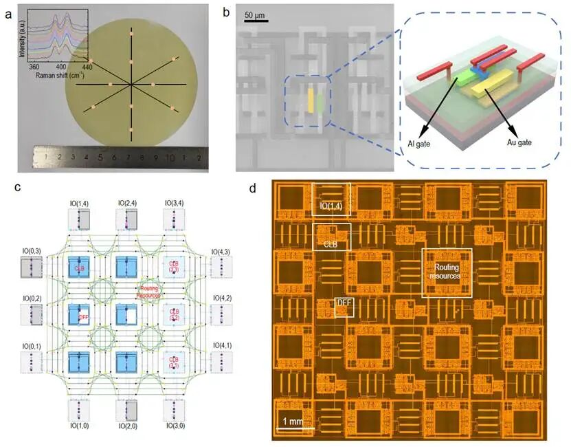
Field-programmable gate array (FPGA) based on two-dimensional transition metal dichalcogenides.(a) Photo of a 4-inch molybdenum disulfide wafer, along with Raman spectra at 10 random locations on a continuous wafer-level molybdenum disulfide thin film.(b) Local scanning electron microscope image of a 2D FPGA unit (left) and a schematic diagram of the 3D structure of E-D type NMOS logic (right).(c) Logic circuit design of the 2D FPGA.(d) Optical microscope image of the 2D FPGA; where CLB refers to configurable logic blocks, I/O is for input/output ports, and DFF represents D flip-flops. (Image source: Shaoxin Laboratory)
1. From “Single Transistor Demonstration” to “System Integration”: Two-Dimensional Semiconductors Overcome the Greatest Technical Barrier
Two-dimensional semiconductor materials (such as MoS₂ and WS₂) are regarded as next-generation ultra-low power, high radiation-resistant materials, but for the past decade, their research has mostly remained at:
- Single transistors
- Small-scale circuits
- Simple microprocessor demonstrations
This time, the FPGA achieved integration of 4,000 transistors and includes:
-
9 configurable logic blocks
-
Nearly 300 configuration bits
-
Logic + storage integration under a unified process (2T cell)
-
Complete reconfigurable logic links (adders, multipliers, counters)
This means that two-dimensional materials havefor the first time broken through“device-level” to“system-level” integration.
FPGA is the“watershed” of semiconductor integration: if it can be done with FPGA, it means the material system has the potential to realize more complex systems (microprocessors, accelerators, AI units).
For two-dimensional materials, this is a milestone leap.
2. Why FPGA? The Best Validation Platform for Two-Dimensional Semiconductors
The choice of FPGA over CPU/GPU is certainly not a coincidence.
The key value of FPGA:
-
Validation of material integrability (at a much higher scale)
-
Logic + storage + routing complexity is higher than that of general microprocessors
-
Extremely high requirements for device consistency
-
Naturally suitable for early material systems to perform“architecture testing”
Traditional silicon-based FPGA has evolved over decades, while two-dimensional material FPGA has completed logic-storage integration in a single wafer, demonstrating the potential of the material system:
- Thinner, lower leakage, more suitable for ultra-low power edge computing
- Extremely high radiation resistance suitable for aerospace missions
- Naturally suitable for electronic systems in extreme environments (high temperature, radiation)
The emergence of two-dimensional material FPGA means:
Two-dimensional materials are no longer“a possibility for the future”, but are on a realistic path to completing complex electronic systems.
3. 10 Mrad Radiation Resistance: Potential to Rewrite Aerospace Electronics
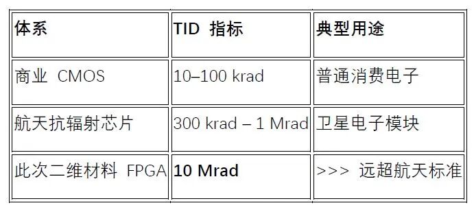
Devices can still operate normally after a total ionizing dose (TID) of10 Mrad, which is a shocking data point.
For comparison:
This natural radiation resistance means:
- Satellites can reduceheavy shielding (protection)
- Satellite electronics payload are lighter and cheaper
- Suitable for deep space exploration and high cosmic ray scenarios
Two-dimensional materials may become key materials for next-generation aerospace electronics.
4. FPGA + Two-Dimensional Materials: Why It Matters for AI and IoT?
Two-dimensional materials FPGA has another direction: low-power edge AI.
FPGA is inherently suitable for:
-
Rapid hardware implementation of AI algorithms
-
Quick validation of custom accelerators
-
Low-power deployment of AI models
And two-dimensional materials themselves:
- Sub-nanometer thickness → extremely low static power consumption
- Absence of traditional silicon short-channel effects → better scaling potential
If larger scales can be achieved in the future:
Two-dimensional materials FPGA could become a new route for“AIoT ultra-low power accelerators.
This is also one of the reasons why European engineers are particularly interested in this achievement.
5. The Overall Layout of China’s Two-Dimensional Semiconductors: Laboratories are Becoming “Systematic Innovation Centers”
This achievement stems from:
- Fudan University: One of the strongest teams in the country for two-dimensional material research
- Shaoxin Laboratory (Shaoxin Lab): A semiconductor innovation platform being developed in Zhejiang Province
Two notable trends:
Trend 1: From material demonstration → architecture-level systems
Following the“Wuji” two-dimensional material microprocessor, this time FPGA indicates:
- The Chinese team is buildinga two-dimensional material system-level roadmap
- From processors → FPGA → the future may be integrated storage and computing, AI accelerators
- Key directions arelogic–storage hybrid integration
Trend 2: Local governments promoting“local trial production” + process optimization“
Shaoxin Laboratory explicitly mentioned:
- The next stage will involveprocess optimization
- Expected to carry outexperimental line validation
This means that two-dimensional material chips may enter:
- R&D samples → small batch validation → custom application fields
Two-dimensional semiconductors are expected to form the embryonic form of a local industrial chain.
6. Returning to Industrial Significance: What Does This Breakthrough Represent?
In summary, the highlight of this wafer-level two-dimensional material FPGA is not in“large scale”, but in:
① This is the first time two-dimensional materials have achieved true system-level integration
FPGA is the threshold of complexity, crossing it means the material system can move towards real systems.
② Natural radiation resistance allows two-dimensional materials to enter“the best candidates for aerospace electronics”
10 Mrad level is a result sufficient to prompt industry institutions to reassess material routes.
③ Potentially disruptive significance for low power AI,IoT, edge computing
Two-dimensional materials can achieve power consumption far below that of silicon.
④ China has shown a leading position in system-level research on two-dimensional semiconductors
Not only producing“material papers”, but also creating“system architectures” and“chip-level engineering”.
⑤ Providing an alternative route to silicon for the potential“post-silicon era”.
If Moore’s Law eventually halts, two types of technologies will become the focus:
- chiplet + 3DIC (the main line for the next decade)
- New material system chips (a longer-term strategic reserve)
Two-dimensional materials FPGA clearly belong to the second category.