A certain audio product’s PCBA (wave soldering process) experienced burning during use. The failure rate was high when using Flux A, slightly decreased after cleaning, and dropped to zero after switching to Flux B. This article will explore the failure reasons through a series of professional testing and analysis methods.
1. Visual Analysis
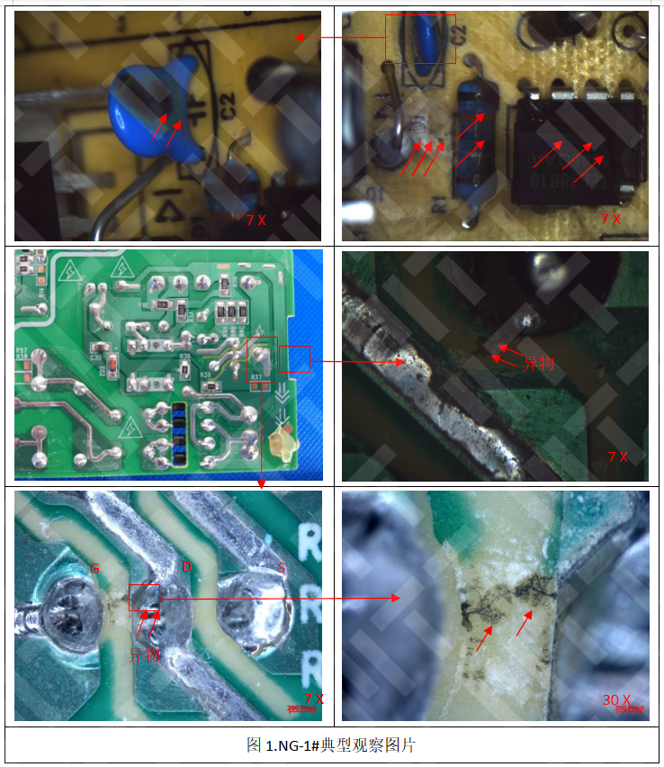
From visual observation, the NG-0# board was the most severely burned, with resistor R1 showing signs of charring and cracking, PWM control chip U1 also burned and cracked, and diode D1 along with resistor R1 and MOSFET Q1 showing burn marks on the PCB surface. Capacitor C2 exhibited slight burn marks; the burning phenomenon on NG-1# board was consistent with that of NG-0#, while cracks were observed on resistor R1 in NG-2# and NG-3# boards. Additionally, foreign substances resembling electromigration were found between the pins on the PCB soldering surface of MOSFET Q1 in NG-1# to NG-3# boards.
2.Electrical Performance Inspection and Analysis
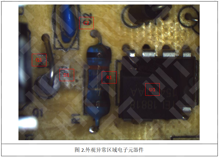
In the NG-0# PCBA sample, the electronic components with visual abnormalities included: MOSFET Q1, diode D1, capacitor C2, resistor R1, and PWM control chip U1 (ITP-LD7535-DIP8).
A. Device Electrical Performance Testing
The PWM control chip U1 has cracked. Electrical performance tests on the remaining related electronic components showed: a short circuit between the pins of MOSFET Q1; the electrical performance of diode D1 and capacitor C2 was not significantly affected; resistor R1 was in an open circuit state.

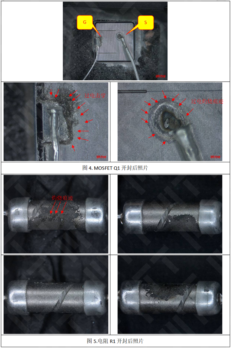
B. Decapsulation Inspection
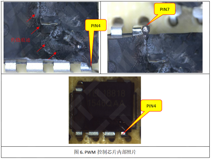
Decapsulation observations were conducted on MOSFET Q1, resistor R1, and PWM control chip U1. The results showed that the insulation layer near the G electrode of MOSFET Q1 was severely damaged, indicating typical over-voltage breakdown, with discharge burn marks also present near the S electrode; the conductive film layer on carbon film resistor R1 had largely peeled off, with burn marks corresponding to the cracks observed during visual inspection; the internal structure of PWM control chip U1 was burned, with the damage most evident at PIN4. Combining the electrical performance tests and decapsulation results, it can be preliminarily concluded that the device damage was caused by overcurrent and overvoltage.
C. Circuit Analysis
The issue focuses on the flyback switch power supply circuit shown in the diagram, with the circuit design directly related to the visual abnormalities primarily including: the snubber circuit and PWM control circuit.
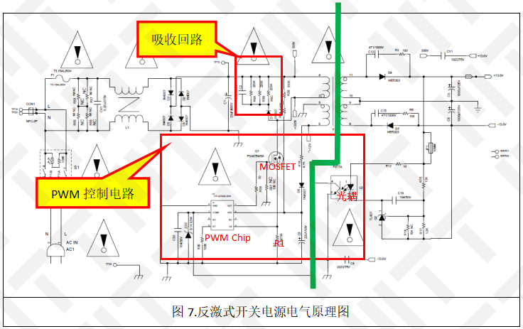
The main function of the snubber circuit in the circuit is to absorb the spike reverse voltage and current caused by the MOSFET during high-frequency operation. If the spike voltage and current cannot be effectively absorbed, it will affect the reliability of the circuit. Inspection of the snubber circuit (including 220K resistor, capacitor C2, diode D1) showed that its electrical performance was normal, and the spike voltage absorption function was not impaired. This indicates that the snubber circuit was not affected and should operate normally.
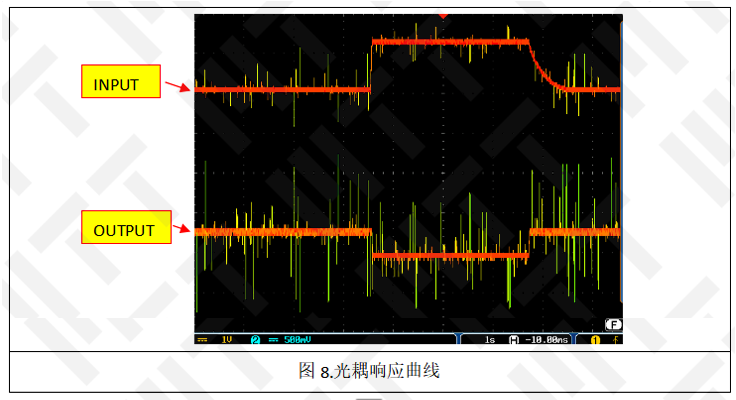
The device damage occurred in the control circuit section, where it was previously analyzed that the direct cause of device damage was overcurrent and overvoltage. The optocoupler is the only device directly connecting the primary circuit (left side of the green line in Figure 7) and the secondary circuit (right side of the green line in Figure 7). Testing the optocoupler to determine whether the overcurrent and overvoltage originated from the secondary circuit showed that the optocoupler was functioning normally (Figure 8), and the possibility of overcurrent and overvoltage occurring in the secondary circuit was very low, allowing us to rule out the influence of the secondary circuit.
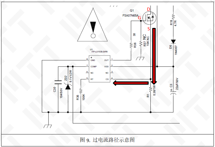
In summary, the circuit analysis can be narrowed down to the section shown in Figure 8. In this part of the circuit, only MOSFET Q1 operates under high voltage conditions. Resistor R1 (0.36Ω/1W) serves to provide feedback and current limiting in the circuit. This resistor was damaged due to overcurrent, indicating that a large current passed through the circuit. Combined with the observation of the most significant damage at PIN4 during the decapsulation inspection, we can conclude that the overcurrent was caused by the breakdown of MOSFET Q1.
3. SEM+EDS Analysis
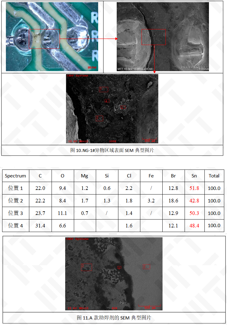
Component analysis of the foreign substances between the G and D pins on the soldering surface of MOSFET Q1 on the failed PCBA board yielded the following results:
NG-1#: EDS component analysis revealed that the main components of the foreign substance were C, O, Mg, Si, Cl, Br, and Sn. Through magnified observation and component confirmation, the foreign substance is primarily tin dross, and the Sn content between the pins on the soldering surface of MOSFET Q1 was very high, while the Sn content in positions away from the soldering surface of MOSFET Q1 significantly decreased. Given that the operating voltage of MOSFET Q1 on this PCBA reaches up to 600V, it is inferred that the cause of the breakdown of MOSFET Q1 was the residual tin dross between the pins.
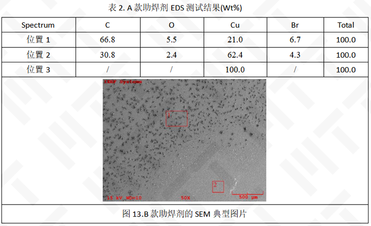
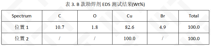
Component analysis of Flux A and Flux B revealed that: Flux A had significant residues on the copper board, while Flux B had minimal residues. The main components of both fluxes were C, O, and Br.
4. Ion Concentration Testing Analysis
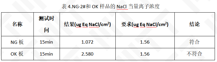
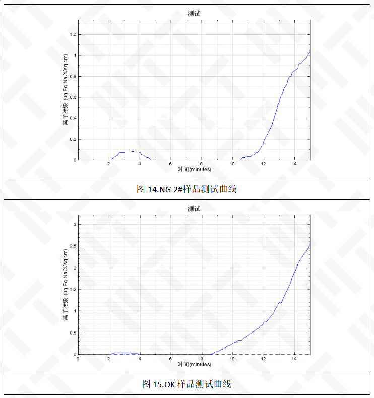
According to IPC-TM-650. 2.3.25C solvent extraction resistivity (ROSE), NaCl equivalent measurements were conducted on NG boards and OK PCBA boards. The results showed that the ion concentration on the surface of the failed board (NG-2#) was 1.072μg NaCl/cm², which meets the standard (≤1.56); the normal board (OK) had an ion concentration of 2.580μg, which exceeded the standard but did not result in burning. This indicates that surface ions are not the primary cause of the PCBA burning.
5. Surface Insulation Resistance Testing of Flux
Surface insulation resistance tests were conducted on Flux A and Flux B. The surface insulation resistance of Flux A was approximately between 1011~1012 ohms, while that of Flux B was approximately between 108~109 ohms, both meeting the standard requirement of greater than 108. This indicates that the ionic residue of the flux is not the cause of the PCBA burning.
The direct cause of the PCBA burning was the residual tin dross between the pins on the soldering surface of MOSFET Q1, combined with the flux residue, leading to a decrease in the PCB’s insulation withstand voltage performance. Feedback from process improvements indicated that after changing the flux, the defect rate significantly decreased, suggesting that the fundamental reason for the board burning was the compatibility issue between the flux and the PCB.
6. Conclusion
The direct cause of the PCBA burning was the presence of a large amount of tin between the MOSFET pins after wave soldering, combined with the ionic residue of the flux, leading to a decrease in the PCB’s insulation withstand voltage performance; the root cause lies in the compatibility issue between the flux and the PCB.


Previous Reviews
|
01 Fire and Burn?! The Real Culprit Behind PCB Corrosive Short Circuits? |
|
02 Breakdown and Burn! This Electronic Component Analysis Report Sounds the Alarm |
|
03 Product Failure Due to Defects in Soldering Process Quality? |
|
04 The Shocking Truth Behind the Blackened Solder Surface of PCBA! |
If you found this helpful, give it a “like”!